
Power Meter - RF Probe

The final performance of the any metering equipment is primarily defined by the characteristics of the transducer device. For an RF power meter, the important attributes are power sensitivity, bandwidth and stability.
The design of this probe is based around the simple Zero Bias Detector, with a Schottky diode as the non-linear element providing power detection. Improvements of the basic design are presented as a way to enhance performance, including a temperature control subsystem and careful construction.
Zero Bias Detector
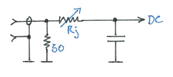
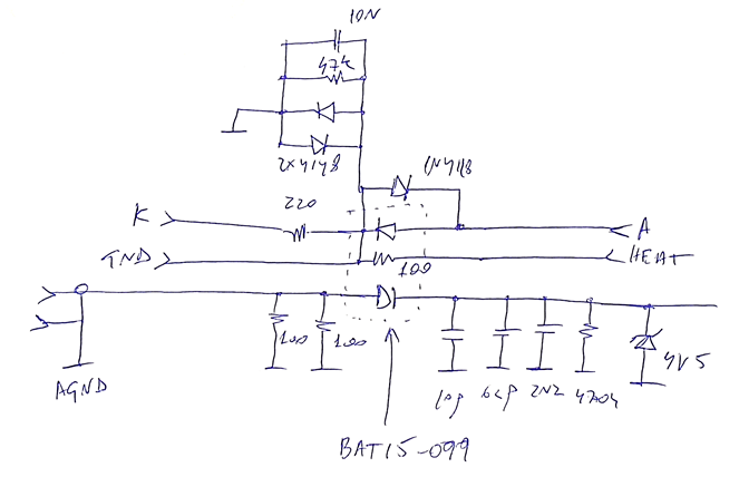
The working principle of a zero-bias detector is the charging of a storage element, the capacitor, through a non-linear resistance element (a Schottky diode) modulated by the RF incident power. For proper operation, the bandwidth at which the resistance can be modulated needs to be higher than the input signal bandwidth (in this simplified schematic, the parasitics that limit bandwidth, as the diode junction capacitance, are omitted).
The resistance Rj represents the small-signal non-linear resistance of a Schottky diode. The incident power at the probe, terminated at the 50ohm input resistor, generates a sinusoidal variable voltage that modulates the junction. Modulation reduces Rj over the positive cycle and increase it over the negative cycles. This resistance imbalance charges the capacitor with unequal current over each semi-cycle, resulting in a DC potential proportional to input amplitude. The output detection signal is usually called video signal.
This small signal behavior extends to very low input powers. Tests with the BAT15-099 diode used in the design shown reliable measurements up to -40dbm. When the input power approaches higher values near 0dbm, the diode starts transitioning to large-signal behavior, working more likely a standard rectifier. Maximum power is limited by the input termination resistors and by the maximum voltage swing allowed over the diode without damage to the junction.
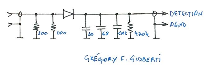
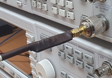
The actual probe circuit utilizes two 100R resistors for proper termination, right at the SMA connector, covering the operational bandwidth with good VSWR. The capacitors are of mixed value to spread the self-resonance effects, increasing flatness. The 10p e 68p capacitors are the main short for the microwave frequencies, and the 2n2 acts as long-term storage and helps with low-pass filtering of the video bandwidth.
All components are of 1206 surface mount type for easy soldering, even though 0805 could result in higher bandwidth and better flatness at band C and band X. The steps of assembly are discussed later in the article.
Detection Response
When the detection voltage is plotted in logarithm scale, the response is close to linear, losing a bit of linearity at higher powers above -15dBm. The overall performance over different frequencies is very similar, presenting small and unpredictable differences (higher frequencies don't generate lower detection amplitude, as some could expect) until the diode low-pass cut-off frequency.
Nevertheless, for absolute accuracy better than 0.5dBm, calibration curves for each frequency of interest are needed. The calibration procedure, automation, polynomial fitting and interpolation is discussed in a different article ??.
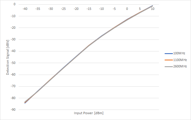
At the lower end of input power (-40dBm) the detected signal approaches -85dBV, that translates to an absolute DC voltages of ~50uV. All aspects in the design of the power meter front-end were to enable the measuring of such small signals with accuracy, stability and repeatability. The final front-end design resembles a DMM circuit, with automatic auto-ranging and auto-zero functions, as discussed in the article Power Meter Front-end.
Heating and Thermal Control
The absolute resistance of the diode junction, represented by Rj in the simplified model, has its magnitude strong related to the junction temperature, thus in directly dependence to the ambient temperature where the probe is used. This strong relation is the biggest obstacle for accurate measurements.
Variations in junction temperature will directly alter the magnitude of the detected signal, making lower power measurements (lower than -15dBm) almost impossible to be made repeatable, degrading the accuracy to ± 3dBm.
The first solution investigated was the measuring of the diode temperature using the second diode inside the BAT15-099 package. When excited with constant current of ~1mA, the junction provide an absolute voltage in proportion to temperature, with -2mV/C. This temperature indication could be used to compensate the calibration curve, if a reliable setup for thermal sweep was used.
Deeper investigation and tests shown that this approach would lead to a difficult and slow calibration procedure and a multidimensional curve-fitting problem, invalidating the idea.
The final design uses a 120R resistor to heat the junction to a stable temperature of ~45C. The second diode junction is used to close the loop with a digital PI controller, precisely ovenizing the probe. The absolute temperature is not of great importance, ensuring that it is stable and higher than normal ambient conditions. Higher temperatures were tested but leaded to thermocouple effects, generating DC potentials in the diode junction and over the cable.
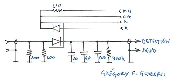
The resistor is soldered to the diode cathode to ensure good thermal connection. In the front-end, a constant current-source of 1mA and a differential amplifier are used to measure the junction temperature in a kelvin configuration, isolating the effects of the heater high currents in the cable resistance.
Assembly
A careful assembly is needed to ensure stable measurements and proper functioning of the heater.
We start with a 40x15mm double-face FR4 board, using soldered copper tape at the 40 mm sides, providing a low inductance connection of both GND planes. A 2 mm centered track is cut using a utility knife.
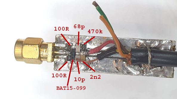
The 100R termination resistors are placed close to the SMA connector, providing good VSWR. A gap is made on the trace to accommodate the BAT15-099, connecting the input side to the capacitors at the right. The two small value capacitors 10p and 68p are connected directly to the diode cathode, assuring good return to ground. The 470k resistor and 2n2 capacitors are then soldered next.
The cable is braced to the assembly using a loop of wire and the copper shield (AGND) soldered to ground. The red (DETECTION) cable carries the detection signal and the others are used for the heater and temperature sensing junction.
Small jumpers made with wire-wrap cable are used to make the other connections, beginning with the temperature sensing diode anode, connected to the yellow (A) cable.
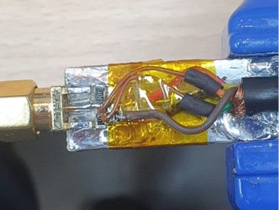
Kapton tape is used to hold the connections firmly and to help with isolation. Tape is used over the diode, leaving only the sensing junction cathode exposed.
Kapton tape is again layered on top of the wires to firmly attach connections, reducing any possible mechanical stress.
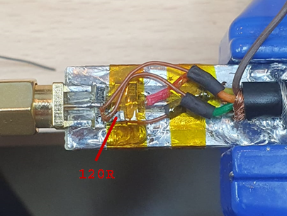
The 120R heater resistor is soldered over the Kapton tape, connected to the diode cathode. Wire-wrap cable is again used to connect the orange (GND) and green (K) cables to the resistor/cathode.
Finally, the brown wire (HEATER) is soldered to the heater resistor.
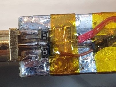
Final touches can now be made to finalize the assembly. I used shrink tube of different sizes to enclosure the probe and to provide mechanical strength to the cable.
Update: 02/02/2022
After real usage on the bench, the probes seemed to have a big problem. After moving the probes over the work or when connecting and disconnecting them from the power meter, they stopped working. One of the BAT15 always got damaged, presenting a short or open, sometimes the detection and other times the temperature sensing junction.
I was certain that the issue was ESD, as the diode got damage even with the probes disconnected, only handling them was enough. After several weeks of tests and with the help of followers from Youtube, we concluded that the issue was an ESD between the diodes, as the two circuits - detection and temperature sensing - didn't share any common connection at the probe.
The probe needed a major redesign.
All components added were placed on the designed for the specific task of ESD protection, with a lot of care to not disturb the well behavior of the probe.
The 47k resistor creates a DC path between the separated grounds, this DC connection requires high impedance to prevent current sharing of the GND lines, that would generate a voltage offset at the detected voltage from the high currents from the heater resistor.
The 10N capacitor help with ESD discharges surges. Any surge that would bring the junctions several volts apart are shunted by the high capacitance, orders of magnitude higher than the equivalent ESD discharge capacitance (the capacitor creates a voltage divider with the ESD capacitance).
Any voltage excursion that is not attenuated by the 47k resistor and 10N capacitor, are hard clamped by the 1N4148 pair, quickly connecting the grounds together, thus equalizing the potential.
A 220R resistor and the 1N4148 protects the temperature sensing diode from reverse voltage spikes, that also would lead to junction damage.
The only change on the detection part of the circuit is the placement of a 4V5 zener, to also prevent reverse voltage on the RF junction. The zener leakage current can be a insue, disrupting the measurement accuracy, tests are needed to guarantee that the temperature stabilization of the probe is enough to also stabilize the zener leakage.
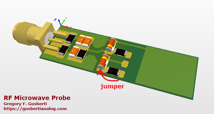
The probes were reconstructed, now with a proper PCB design. I made the boards in my lab using toner transfer. The upper diode is the output zener. Some components are placed on the bottom of the probe, to keep the overall size similar to the original.
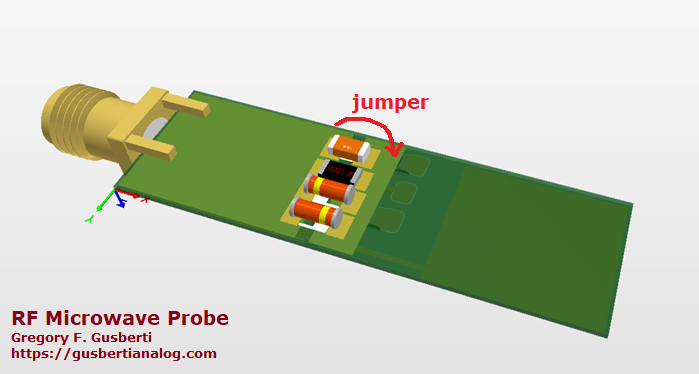
To facilitate the construction, I used a jumper to connect the grounds together. The jumper runs on the side of the PCB, without the need of a via, that is difficult to make at the homelab. Unfortnely I don't have any picture of the construction steps.
The probe is running fine now and the Power Meter + Probe has being an amazing tool on the lab.
References
+ https://www.spelektroniikka.fi/kuvat/schot17.pdf
+ http://www.hp.woodshot.com/hprfhelp/4_downld/lit/diodelit/an1090.pdf
+ https://www.infineon.com/dgdl/Infineon-AN_1807_PL32_1808_132434_RF%20and%20microwave%20power%20detection%20-AN-v01_00-EN.pdf?fileId=5546d46265f064ff0166440727be1055
+ https://g3ynh.info/circuits/Diode_det.pdf
+ https://g3ynh.info/circuits/Diode_det.pdf
+ https://www.rf-microwave.com/app/resources/uploads/diodes/AN923.pdf
+ http://www.dl5neg.de/diodesensor/diodesensor.html
+ https://www.analog.com/ru/technical-articles/measurement-control-rf-power-parti.html