
Power Meter - Front-end and Digital Section
As explained in the article about the RF Probe, the main task of the power meter device is the precise measurement of voltages over multiple decades, conversion to the calibrated measured value and control of the probe heater. In this article, we discuss the working principles of the front-end design that enables more than 50dB of dynamic range and general aspects of the remaining subsystems.
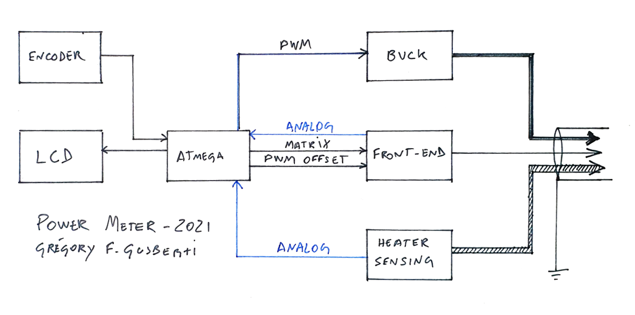
A central ATmega328 microcontroller commands all behaviors of the device and is responsible for the conversion of the analog values using its internal 10bit A/D. An analog front-end buffers, amplifies with different gain ranges and allows auto-zero function. The gain matrix allows gains of 1x, 22x and 470x, enabling the conversion with 5 decades of dynamic range, oversampling and digital low-pass filtering increases even more the resolution.
For reducing costs of implementation and difficulties in hard to find parts, a PWM D/A provides offsetting voltages to the front-end main operational amplifier. This enables the usage of not so expensive parts, as voltage and input bias offsets are null on startup.
The probe heater and temperature sensor demands its own analog section, containing a 1mA biasing current-source and a differential amplifier for measurement of the junction voltage. The kelvin connection right at the BAT15-099 eliminates errors from voltage drop on the cable, generated by the high currents of the heater resistor.
A discrete buck-converter controlled by PWM powers the heater resistor with variable voltage. The microcontroller utilizes a digital PI loop to stabilize the temperature of the BAT15-099 by adjustments on the heating level, utilizing the sensed voltage from the differential amplifier.
The ATmega328 also controls the 40x02 character LCD and reads the quadrature signals of the encoder, providing a responsive user interface that runs in parallel with the measuring and calibration DSP. Multiprocessing is provided by a cooperative software architecture, where different subsections of each "process" are split apart in state-machines and elapsed time counters.
Main Front-end
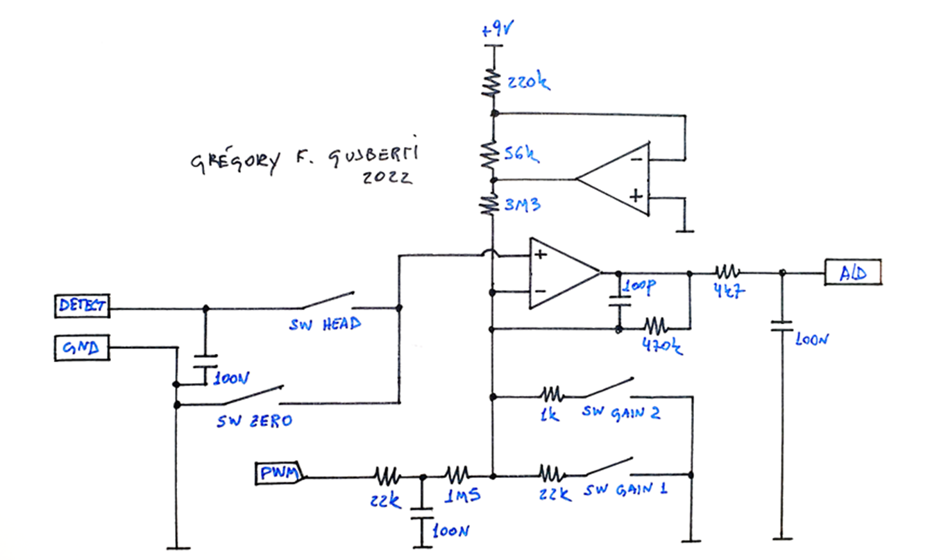
The task of the analog front-end is the amplification and conditioning of the DC signal generated at the power-meter probe, and its performance directly imposes the bottom limit of the dynamic range.
At lower input powers, the probe generates detection voltages of microvolts, thus the main concerning of the design is a low (and stable) voltage offset in the main amplifier. To allow the usage of a jellybean FET input opamp, the circuit contains an input matrix of analog switches, SW-HEAD and SW-ZERO and a controllable bias network.
At start-up, the microcontroller performs an initial offset cancellation using a filtered PWM as a DAC. The upper opamp generates a stable negative bias that introduces a positive offset on purpose, through the 3M3 resistor, almost bringing the opamp into saturation. This topology enables a positive voltage, generated by the PWM DAC, to bias the opamp to a zero-offset condition.
At operation, the input switch matrix allows the AVR to measure any remaining offset voltage, periodically performing an auto-zeroing, like in modern DMM circuits. This relaxes the need for precision low-offset opamps and compensates for any drift in the overall circuit.
Two analog switches, SW-GAIN-1 and SW-GAIN-2, are used to switch the gain of the amplifier, allowing auto-ranging. The AVR firmware continuously checks if a range change is needed, preserving the maximum resolution possible at the measured signal.
The opamp is compensated for stability, and the output signal is further low-pass filtered before digital conversion. The A/D 10 bits resolution is enhanced by oversampling and digital filtering in the firmware DSP stack.
Probe Heater - Bias and Sensing
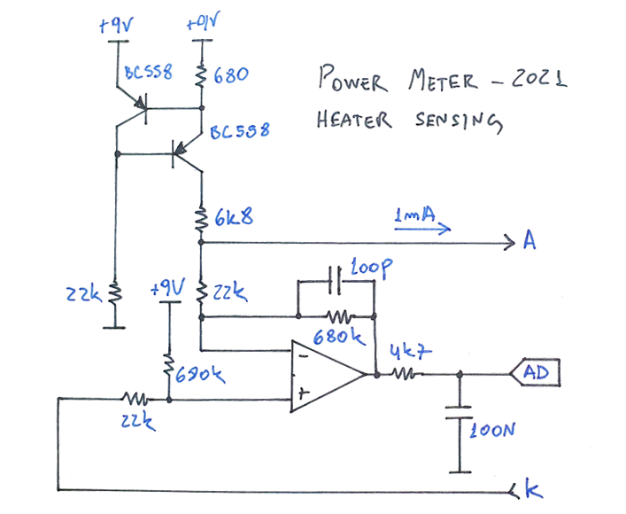
The diode junction used for sensing is biased by 1mA through Q1 and Q2 current-source. The opamp works in differential mode, amplifying the junction voltage sensed by the kelvin connection scheme.
The differential gain is configured to ~31x, sufficient to reach enough resolution from the 10bit A/D. The nominal voltage of the BAT15 junction at ambient temperature, close to 245mV, is offsetted using the same resistive gain network.
The output is low-pass filtered before reaching the microcontroller helping in two ways, preventing high frequency noise from affecting the analog conversion and also blocking any ATmega internal noise from affecting the analog front-end section.
The filter series resistor also allows the microcontroller internal input clamping diodes to work properly, protecting the A/D input from any voltage excursion higher than 5V (unpredictable voltage excursions could result from probe disconnection, or extreme sensed temperatures, as the opamp is supplied with 9V).
Probe Heater - Buck-converter
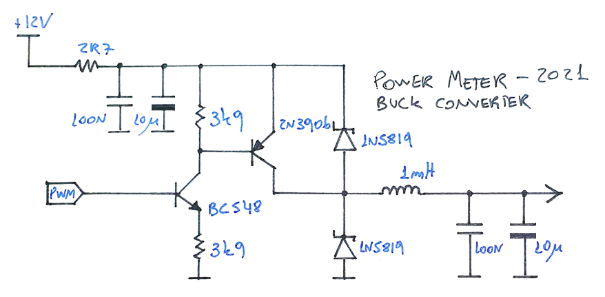
The 120R resistor used as the heater element on the probe needs currents as high as 80mA, thus a small DC-DC converter was designed to allow control of the heating. The design is based around the common buck-converter, using jellybean BJT transistors and Schottky diodes.
The first design concluded that proper filtering of the DC-DC converter output is needed, as switching ripple couples in the analog lines through the long cable, degrading the measurements in the uV range, thus forbidden the usage of a simpler PWM chopper as tested in the first attempts. The conventional buck-converter with LC output filter solved this issue, nevertheless, in a future design, a cable with separated shielding for the analog lines would be a better choice.
The ATMega 5V PWM signal is level-shifted by Q3, providing a proper voltage swing for Q4, the main converter switch. The two freewheeling diodes are common 5819 Schottkys. Low-pass filtering is accomplished by the LC output filter, using a 1mH choke inductor and combination of electrolytic and polyester capacitors. A true inductor (not of choke kind) would be a better choice, reducing the power loss on the converter.
The power supply for the converter is tapped from the 12V through an RC low-pass. The filter slightly reduces noise coupling and helps to limit the current in fault conditions.