
Frequency Multiplier with PIN diode
In this article we are going to discuss and prototype an old technique used for high frequency synthesis, that for many years was the only way to approach tens of gigahertz.
PIN diodes have a large signal behavior, very similar to step-recovery diodes. Even with SRD becoming expensive and hard to find, PIN diodes are used almost in all microwave systems today.
The working principle is simple from a block diagram perspective. In this prototype, a 100MHz signal is largely amplified and applied directly to a PIN diode. The large signal behavior of the diode is excited, generating fast current spikes at the input frequency. This high energy pulse train is rich in harmonics, allowing a band-pass filter to isolate the frequency desired at the output.
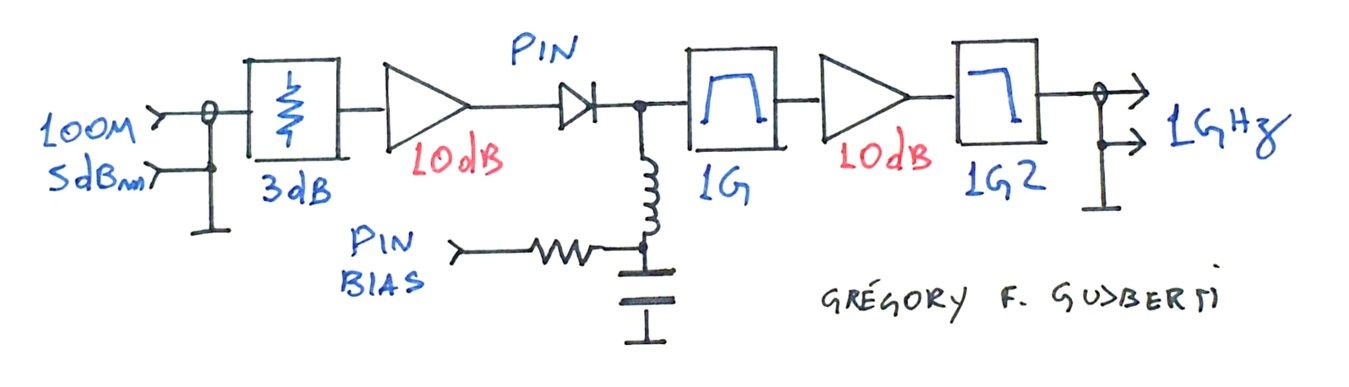
The band-pass filter necessary to isolate the desired harmonic will have high insertion-loss when designed with microstrip topology in FR4 material, as the needed bandwidth is narrow. To compensate the filter loss, an output tuned amplifier provides a higher power signal at the output.
The low-pass filter has low order and helps to attenuate slight the strong 2nd and 3rd harmonics generated by the output amplifier compression.
PIN Diode Large-signal Behavior
The PIN diode large-signal behavior has a strong step-recovery characteristic. When RF signal swing is sufficient for forward conduction, the PIN diode works as a rectifier diode, presenting low dynamic resistance and a constant junction voltage drop.
The step-recovery action appear when the PIN diode enters reverse bias. The high carrier recombination time provided by the "I" region allow reverse conduction until all the charges are recombined. At the moment when all stored charge recombine, the impedance quickly becomes orders of magnitude higher, collapsing to the reverse bias state.
This fast transition of the reverse bias impedance is what provides the fast pulses of energy that are rich in harmonics.
Circuit Description
The circuit was designed and assembled using my preferred microwave prototyping technique, using copper tape over an FR4 single sided PCB.
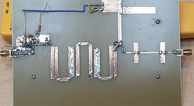
Low inductance vias are made using 3.5mm drilled holes, with the bottom side covered by copper tape. The holes are after filled with solder, providing a strong ground connection to tens of GHz. Transmission line connections are made with ~2.8mm width copper tape for 50ohm impedance. The width can be increased or reduced, allowing the impedance changing necessary for more complex microstrip architectures.
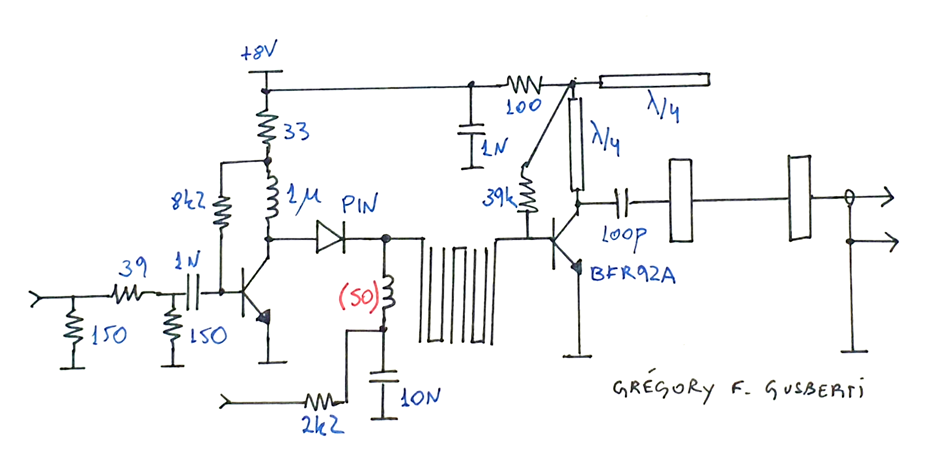
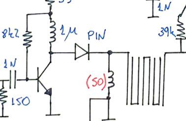
The circuit input is present on the left side of the circuit diagram. Right at the input, a 3db pad is used to reduce signal reflection from the unmatched BJT base. The input amplifier is biased with 50mA, attaining more than 10dB of gain at 100MHz.
The PIN diode is directly coupled to the amplifier collector. It is very important to shunt the signal at the diode end, providing the path for the high current exciting signal. This is provided by the inductor and capacitor after the PIN diode, that also couples the DC biasing voltage to the diode.
In red and in parentheses is the reactance of the inductor at the desired output frequency. This places the 3db cut-off near the desired harmonic, shunting the energy of lower frequencies to ground, as the inductor reactance will be lower at lower frequencies.
Combined with the band-pass filter, the current returning path works like a diplexer network, allowing the desired output frequency to pass through, reaching the next amplification stage, while the exciting 100MHz energy is returned to ground.
The second amplifier is tuned at the desired output using two quarter-wave transmission lines. The high insertion-loss is compensated and further isolated by the tuned behavior of the amplifier. If better output impedance termination is needed, it is recommended to use one more amplifier, designed for broadband 50ohm impedance, like that of the ERA series.
A stepped impedance low order low-pass filter is used right before the output connector to reduce the harmonic distortion generated by the second amplifier compression. I used a 3rd order filter because it was the higher order that fitted at my prototype. In a better designed system, I recommend a minimum order of 5th.
Band-pass Hairpin Filter
My initial experiments started with edge-coupled microstrip filters. They seemed of easy tuning and design, working great for homemade projects.
I switched to the Hairpin topology because of the reduced width profile, fitting in the PCB I used. Each section of the filter have an approximated height of lambda/4 and the separation is increased in the middle section, providing higher loaded Q thus narrow pass-band.
Tuning is possible by increasing or reducing the length of each resonator, using small pieces of copper tape. In a final design, I would also test comb or interdigital topologies, but the need for right placed vias make prototypes infeasible.
PIN Diode Bias
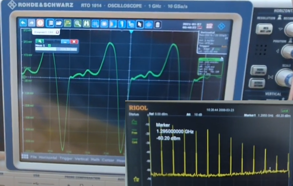
For proper step-recovery behavior, the choice of the bias current is crucial. It can be seen in this video how the harmonic distribution changes as the bias is modified. I connected a separated voltage supply at the bias voltage input, allowing the voltage to be tuned. The proper voltage is that one that maximizes the output power at the desired output frequency.