
BJT PN Junction Noise Source
Reverse biased base-emitter junctions are effectively used as noise sources, with a great amount of ENR (Excess Noise Ratio) originating from the intrinsic behavior of avalanche and zener operation.
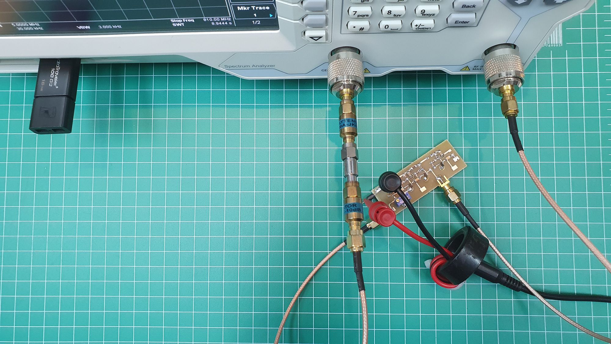
This article is a compilation of measurements in a noise source prototype - designed for evaluation of a subcircuit for another design - with different models of common RF transistors.
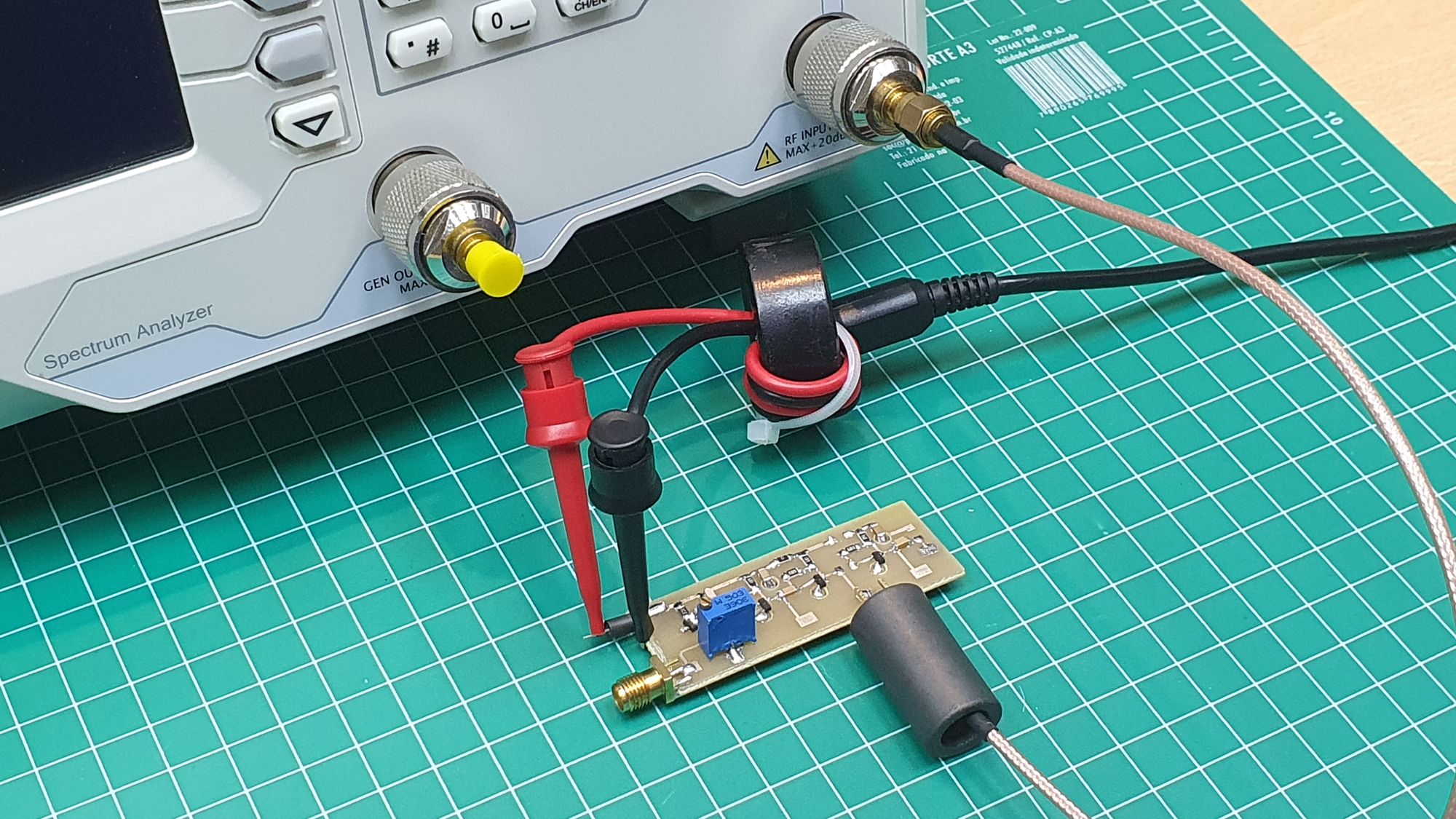
The prototype PCB was etched in common 1.6mm FR4, using 3mm drilled holes serving as solder filled vias.
A chain of tree amplifiers follow the noise generator BJT, amplifying the noise to useful output amplitudes. The chain was designed for easy disconnection of the stages, where the number of amplification steps needed was chosen experimentally. The tests were all performed using only the first two stages, as they presented the needed output level.
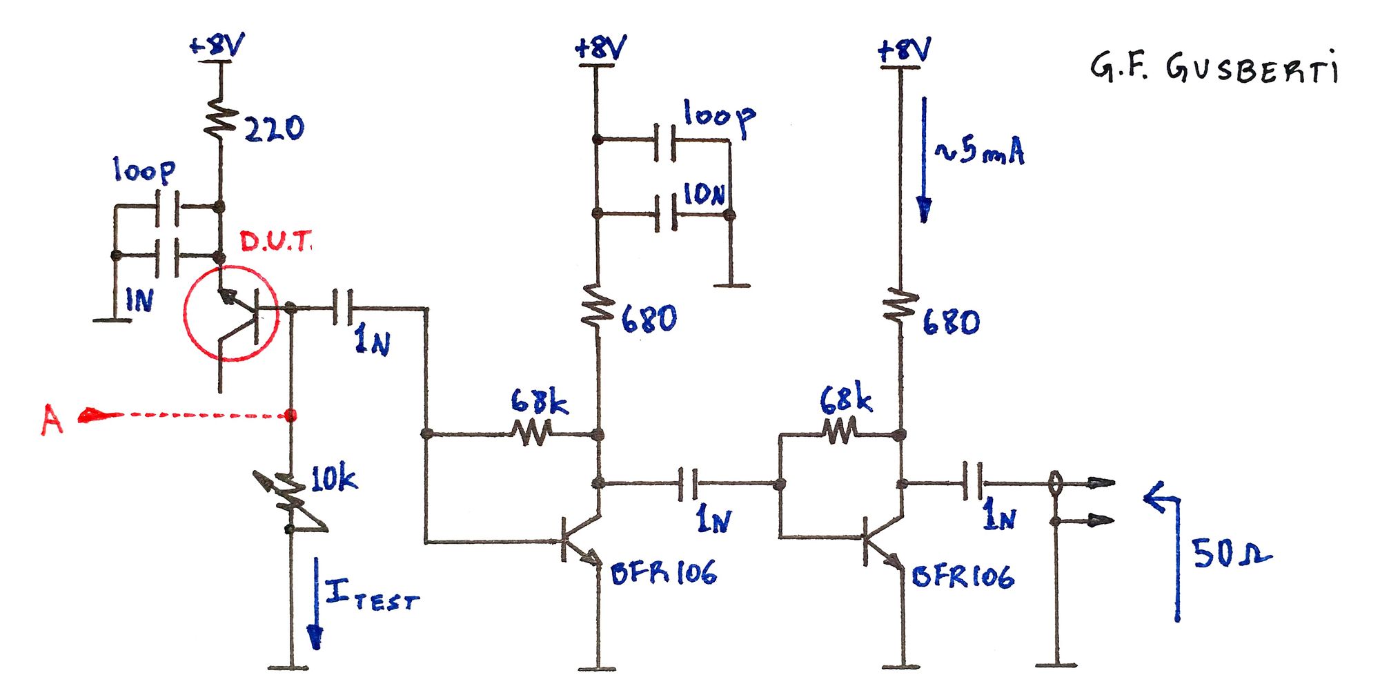
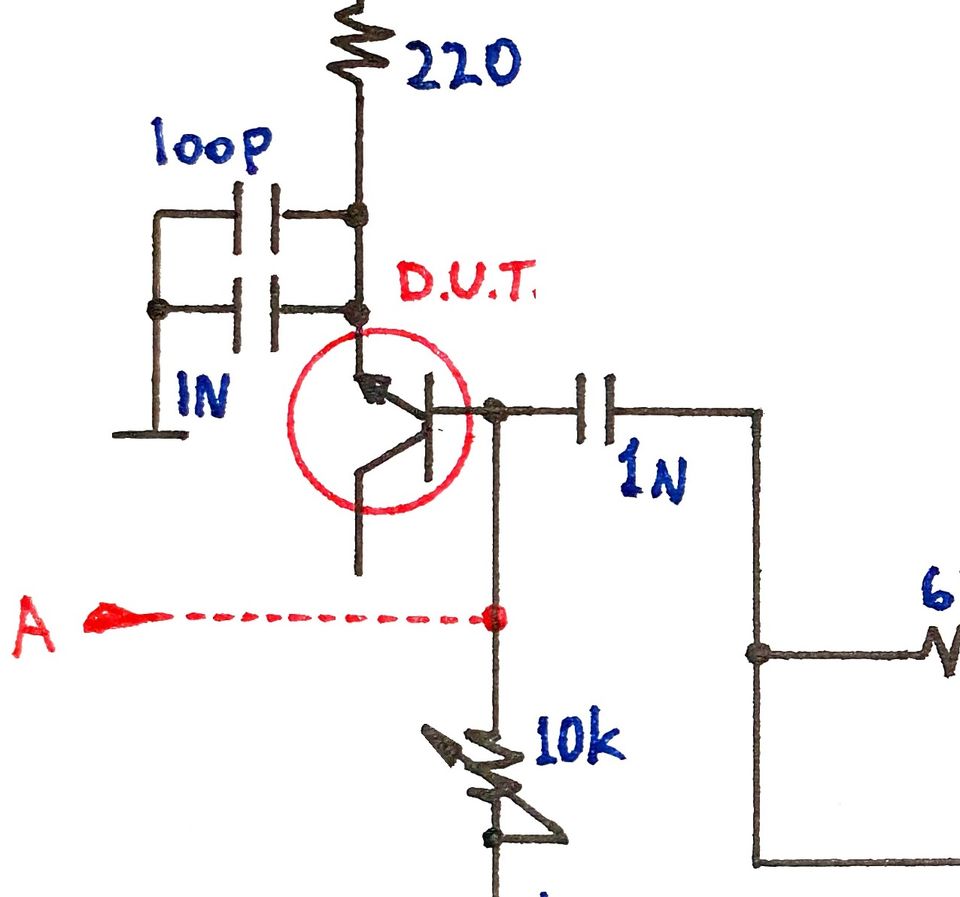
The noise generator BJT has its base reversely biased, using a trimpot for setting the quiescent current. The signal at the base is AC coupled to the first amplification stage.
The amplifiers are very simple BFR106 common-emitter stages, without any feedback compensation for flatness, biased at ~5mA each. The assembly is powered by a single 8V DC connection.
Noise Generator
The reversed biased base-emitter junction operates in a combination of Zenner Effect and Avalanche Breakdown, with a reverse voltage of ~4.5V to ~5.5V. The intrinsic noise generation happens by quantization of charge, as electrons jumping through the junction potential carry integer multiples of charge quanta.
The flow of discrete charge amounts across the potential barrier fluctuates randomly, modulating the reverse voltage across the junction, with a white noise spectral density. Flicker-noise and excess noise - generated by avalanche - enhance the noise profile of the reversed base-emitter junction.
Measurement Setup
For speeding up the capture of data and for guaranteed repeatability, a measurement setup was designed, using a DSA815TG spectrum analyzer, aided by software automation.
For each measurement, software resets the SA and presets the equipment for: RBW = 30 kHz, VBW = 3 kHz, detector = sample, Trace AVG Count = 6, Trace AVG Mode = Power, 5 MHz to 810 MHz span, Maximum Mixer Level -5 dB, internal 20 dB pre-amplifier ON.
This setup was chosen experimentally by looking for the lower noise-floor possible, while still maintaining enough dynamic range for the measured signal.
After the trace averaging completes, the sweep is paused and a Noise Marker is swept over the final trace, from 10 MHz to 800 MHz, in 10 MHz steps, storing each noise density point in the dBm/Hz scale.
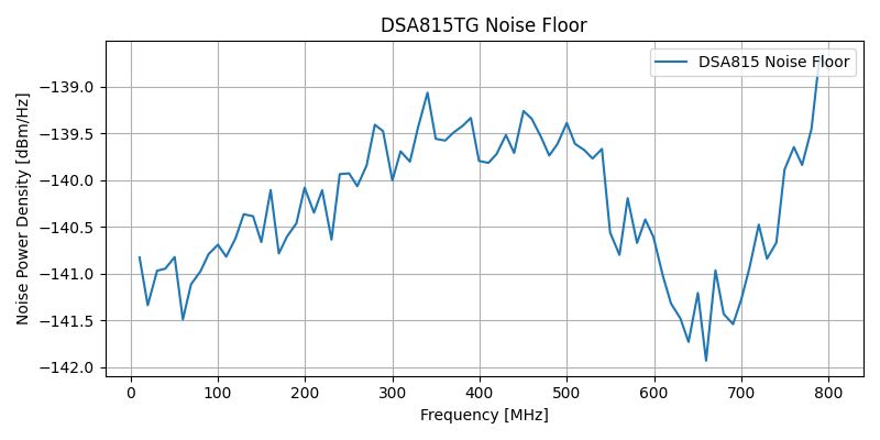
The noise floor of the SA was also captured, connected to a 50 ohm load at ambient temperature, with the intention of de-embedding its own noise temperature from all the BJT measurements.
Measured Noise
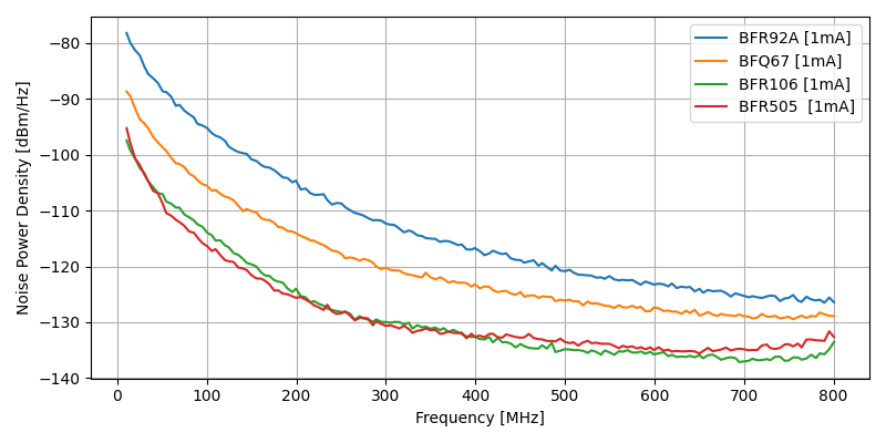
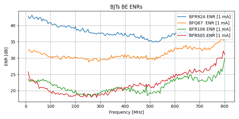
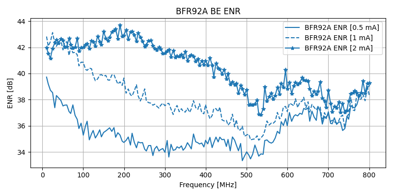
Four SOT-123 RF transistors were measured - BFR106, BFR505, BFR92A and BFQ67 - using three reverse quiescent currents of 500uA, 1mA and 2mA. Higher currents were found difficult to maintain stable and did not show higher noise profiles.
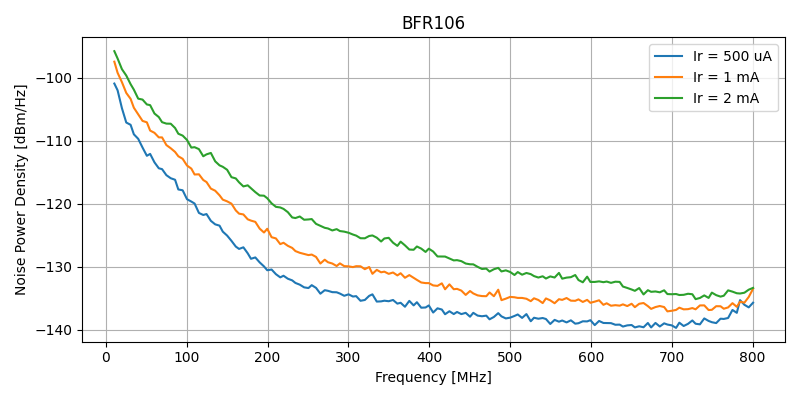
The measured noise density has a fast roll-off from 10 MHz to 200 MHz, an effect mainly generated by the gain slop of the amplifier chain. The noise profile flattens a bit, with a reduced slop up to the end of the frequency span. The small rise near 800 MHz happens by environmental noise, inadvertently coupled into the measurement, mainly from strong signals in the cellular band.
Out of curiosity, the gain profile of the amplifier chain was de-embedded from the measurements, at the end of this article. However, these are the data points needed for proper characterizing this noise source module, as it will be used - with the amplifiers - as a subcircuit in another design.
The remaining measurements are demonstrated at the end of the article.
Setup Noise Floor
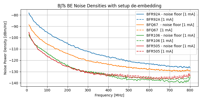
For a proper Excess Noise Ratio characterization, the collected noise density measurements need to be subtracted by the setup own noise temperature, as the noise marker is actually measuring the temperature of the SA internal electronics + the external signal.
To perform this correction, both measurements - SA noise floor and target BJT noise - are transformed to linear noise temperatures - in the Kelvin scale - and are then subtracted. The result is then converted back to power densities in dBm/Hz.
When comparing the raw measurements with the corrected ones by the noise floor, it is possible to see that the correction affects much more the noise densities measured at higher frequencies. This happens as the BJT junction generated noise approaches the noise floor of the measurement setup, as seem below.
ENR and Amplifier Chain De-embedding
Estimating the Excess Noise Ratio of the base-emitter junction becomes possible by first de-embedding the power gain of the amplifier that follows the noise junction. For this experimentation, a SMA connector was soldered at the BJT position (A test point in the schematic), exciting directly the input of the first amplifier transistor.
For the high gain expected by the two common-emitter amplifiers, 40 dB of attenuation was added to the -20 dBm excitation from the SA Tracking Generator. The low signal level prevents performing the measurement near (or above) the compression point of the amplifier.
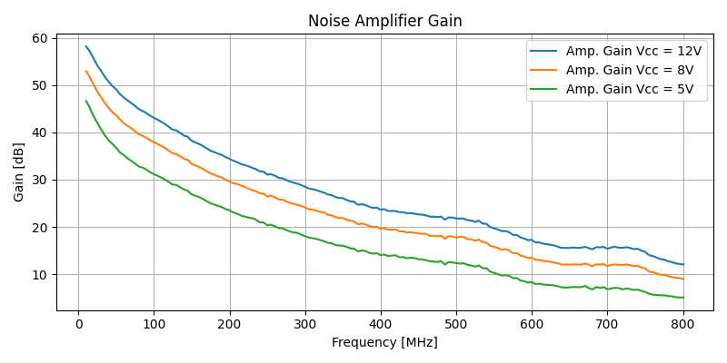
It becomes evident that it is the frequency response of the amplifier chain what shapes the noise density of the overall design. The design utilizes 8V as the Vcc voltage.
Subtracting the measured gain from the output noise density (already corrected for the setup noise temperature), we arrive at the amplifier input referred noise density that - neglecting the PN junction impedance mismatch and the amplifier own noise figure - approximates the noise density generated by the PN junction.
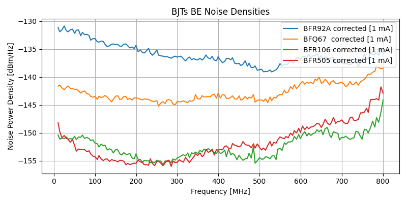
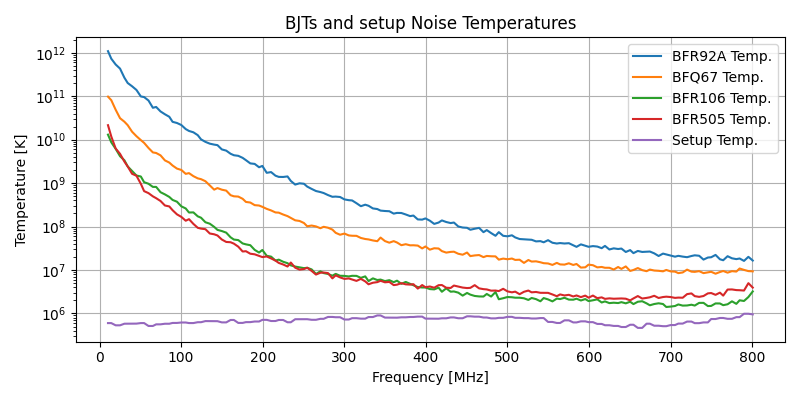
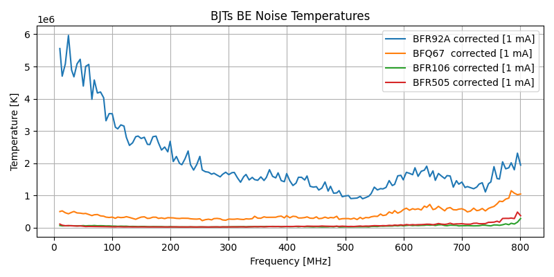
These are the BJT reverse-biased base-emitter PN junction Noise Power Densities. The same result can be displayed as Noise Temperature (for 1 Hz bandwidth), as below.
The Excess Noise Ratio (ENR) - measuring how much the noise is above thermal - is computed directly from the temperatures, as follows.
As expected for ENRs > 15 dB, these computed ENRs could be approximated by subtracting the thermal noise floor of -174 dBm/Hz from the measured noise densities from the reverse-biased junctions.
The ENR of the BFR92A for different reverse currents shows an increase in magnitude for higher currents, agreeing with the expected behavior.
PN Junction Bias
The base-emitter junction should be biased in reverse, with a stable constant current. The simple prototype described here could be improved in this aspect.
The constant current assumption, used by the biasing of the junction with a constant voltage plus a series resistor, is far from ideal. With 8 V as VCC and a reverse voltage drop of ~ 5.5 V, the voltage left over the resistor stays around 2.5 V, giving poor current stability to the system.
This would not be the case for higher supply voltage, like 24 V, as the majority of the voltage would be burned over the resistive drop, operating the circuit closer to a constant current.
The practical effect, observed with the prototype, was difficulty to maintain the current stable, and presence of runalway for currents greater the 2 mA.
Formulas
Noise Temperature = 10 ^ (([Noise Density] - 30) / 10) / Kb
Noise Density = 10 * log10 ([Noise Temperature] * Kb) + 30
ENR = 10 * log10 ((T - 290) / 290)
Where T is temperature in Kelvin, Kb is the Boltzmann constant. Noise temperature always relative to 1 Hz bandwidth.
References
https://en.wikipedia.org/wiki/Noise_generator
https://en.wikipedia.org/wiki/Shot_noise
https://byjus.com/physics/difference-between-zener-breakdown-and-avalanche-breakdown/
https://cr4.globalspec.com/thread/72501/Emitter-Base-Breakdown-Voltage-of-NPN-Used-as-Zener
https://www.analog.com/en/technical-articles/noise-figure-measurement-methods-and-formulas--maxim-integrated.html#:~:text=In%20terms%20of%20Noise%20figure,with%20the%20Y%2Dfactor%20method.