
Clock Recovery with digital PLL
In digital communication, where data messages are transmitted encoded in bitstreams, the receiver end is always presented with the challenge of clock recovery.
Clock recovery is the art of reestablishing the time slices of the encoded bits, that were generated in the transmitter side. This timing information, for NRZ signals, is not transmitted, because it would occupy bandwidth without payload information.
NRZ Signal
NRZ (Non-return-to-zero) encodes the bitstream in the level of the line signaling. Usually, a high level (positive voltage or higher light intensity in optical links) represents a 1 and, a lower level, a 0 bit.
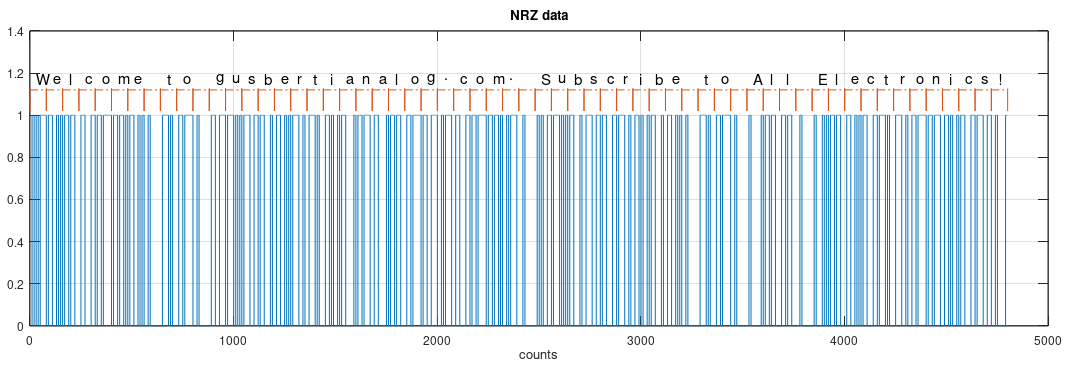
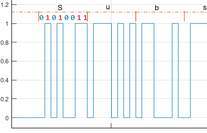
In this example we have a payload message, encoded using ASCII, where 8 bits represents each letter, which then modulates the level of the line, generating the NRZ signal.
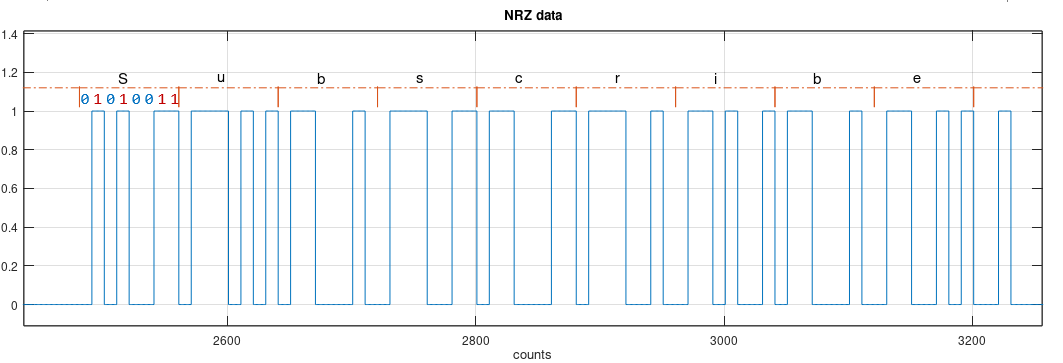
The ASCII standard defines the letter S (uppercase) as the binary sequence 01010011, that is easily seen represented in the level of the line.
Decoding the NRZ encoded bitstream
To decode and interpret the received stream, the receiver end needs to precisely decide when to measure the level of the line, to recognize the zeros and ones. Looking at the picture of the signal, by the human eye, the decoding step looks easy, but it is an optical illusion because we are seeing the full frame of data.
A real receiver cannot look into information that still not arrived, and need to make decisions using only the current level of the line and past transition.
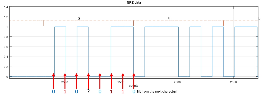
If the receiver is detecting the levels with a slight error of frequency or phase (it starts detecting before or after the ideal timing), the transmitted information is totally lost, as easily seem in the picture.
A mechanism to recover the ideal timing, keep tracking of changes in relative frequency and phase, is needed. This is the job of the Clock Recovery System.
Clock Recovery System
The only aspect we have, that carries part of the timing information, is the transitions between different bits. As we are going to see, transitions alone don't delivery a full solution, and a more complicated recovery system is needed (think with me, the sequence 1111, as an example, don't have any transition!).
The spectrum of a level encoded signal is a sinx/x function in the frequency domain.
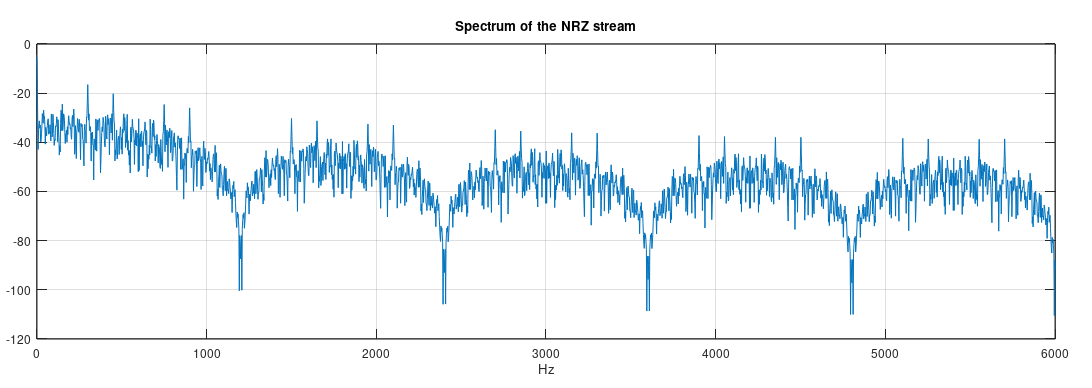
The signal has its power spread in a wide bandwidth, without much information about the bitrate. The only interesting visual aspect is the notches, evenly spaced apart. The first one happens to be exactly at 1200Hz, the bitrate of the simulated signal (1200 bits/s).
The energy being spread in frequency is actually the mathematical explanation about why it is hard to decode the signal. A large bandwidth signal is the dual of a well positioned information in the time-domain. This aligns with the conclusion that the timing information is only well presented in some parts of the signal - in its transitions - and not in the overall bitstream.
A better time-domain information about the overall bitstream will appear, in the frequency-domain, as power concentrated in specific frequencies.
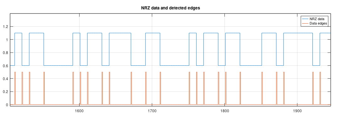
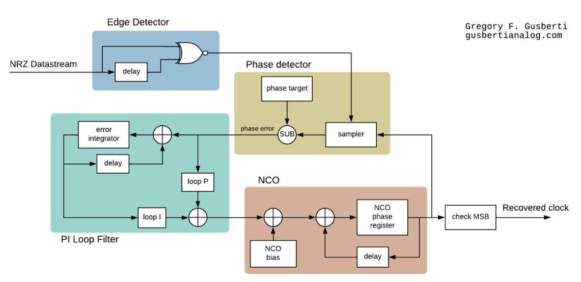
Here we are able to use a simple but clever trick, and the first step at the receiver Clock Recovery System, is the processing of the signal through an edge detector.
The edge detector generates a signal with pulses exactly at the transitions of the received NRZ stream. This has the interesting effect of collapsing the sinx/x spectral energy into well localized frequency spurious.
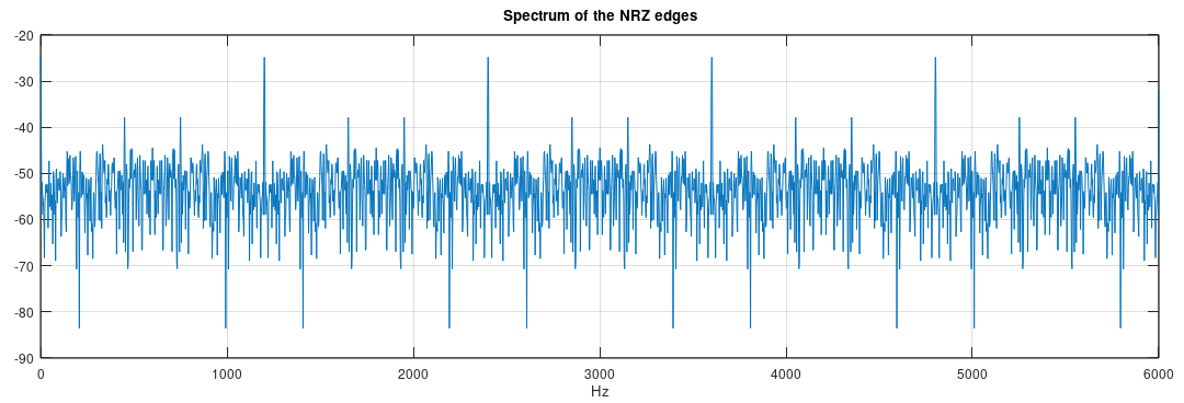
The first frequency component is precisely at the bitrate frequency, 1200Hz. This is the base for clock recovery, where a timing generator will lock at this spectrum line, generating the periodic sampling of the signal line. It is useful to have a system where the phase of the generated clock is adjustable, to be correct aligned to the ideal decision moment.
The mechanism that is capable of frequency and phase locking, that is adjustable, compact and narrowband is the PLL (Phase-locked-loop).
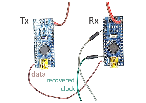
The PLL designed is entirely digital, and a prototype was programmed in an AVR microcontroller, for tests in the bench.
The input to the PLL if the edge detector, working as a XOR gate. The gate detects transitions of the NRZ bitstream, comparing its current level with a delayed version. In the case of different levels, an edge is acknowledged to the phase detector.
The phase detector is responsible for detecting differences in the phase/frequency of the edges and the periodic signal generated at the NCO. Every time a phase difference is encountered (the NRZ edges are late of before the edges of the NCO), the phase error is calculated, subtracting the desired phase from the current phase.
The error signal is filtered with a PI controller. Filtering is necessary to average the error over time and to compensate the response of the closed loop, generating a stable control word for the NCO.
NCO stands for Numeric Controlled Oscillator, and is the digital counterpart of the analog VCO. This oscillator will become the local time reference of the receiver, generating transition edges exactly at the ideal time of decision. Any time the phase comparator detects a misalignment of the incoming NRZ edges and the NCO, the error propagates through the PI filter and compensates the NCO, bringing it back to tick in time.
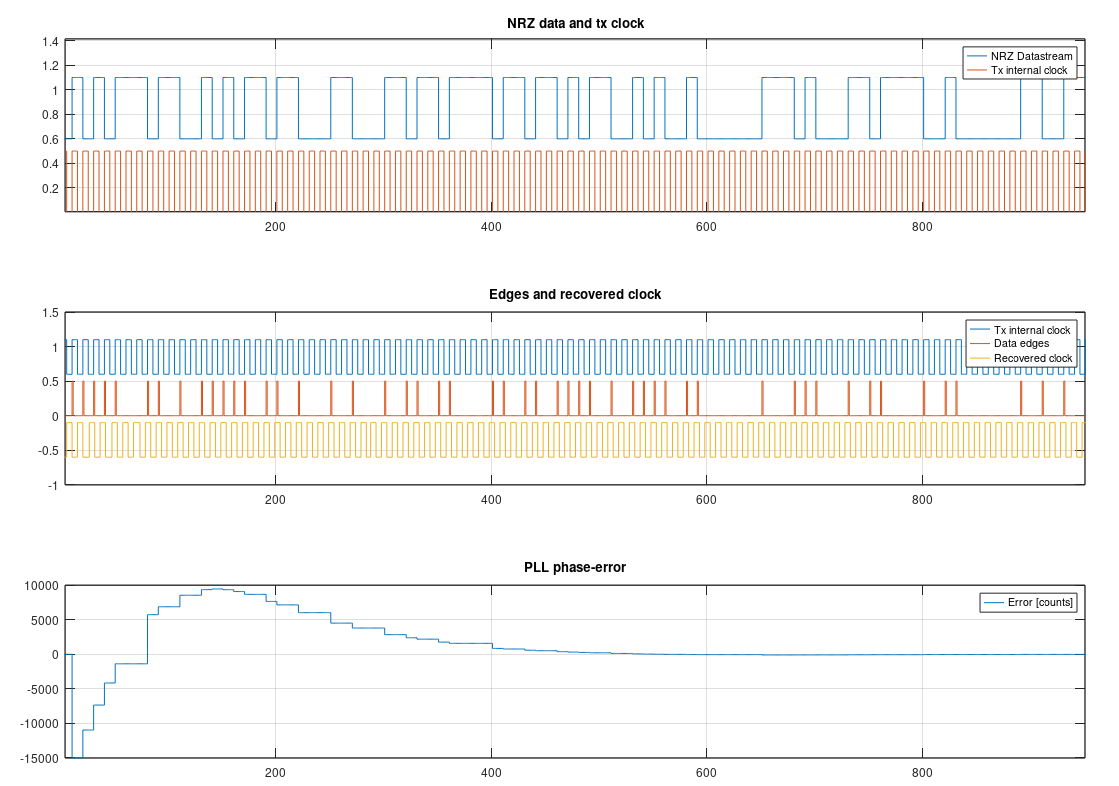
The upper plot shows the NRZ data and the clock signal available at the transmitter (the clock that generated the NRZ levels). The transitions of the NRZ data happens in sync with transitions of the transmitter clock, as this clock is the time base of the Tx.
We see clearly that each bit has it own clock transition, and this only exists at the transmission side. As you saw early, only the bitstream is sent, and the challenge is to recover the ideal clock only looking at the available transitions in the data.
The middle plot shows the PLL Clock Recovering working. The orange trace is the edge signal, detected from the received data, and the yellow trace is the output of the NCO. The numeric oscillator generates a signal exactly equal to the transmitter clock, using only the edges as reference, never seeing the original Tx clock. The transmitter clock, in blue, was printed only for comparison.
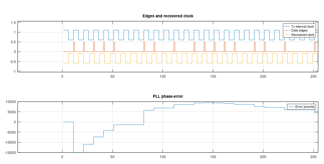
In the beginning, the phase error, at the input of the PI filter, is high, because the NCO starts running at a different phase/frequency than the timing of the data. The closed-loop readily corrects the NCO, bringing it in lock with the signal.
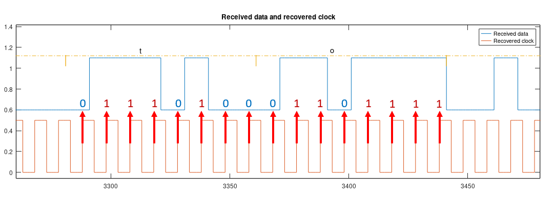
Now, to correctly decode the bitstream, the receiver needs to measure the level of the line in sync with the recovered clock. In this simulation, the PHASE_TARGET parameter of the loop was set to 90 degrees. This generates a recovered clock 90 degrees later than the transition of the bits, ensuring the correct detection of the bits.
Frame sync
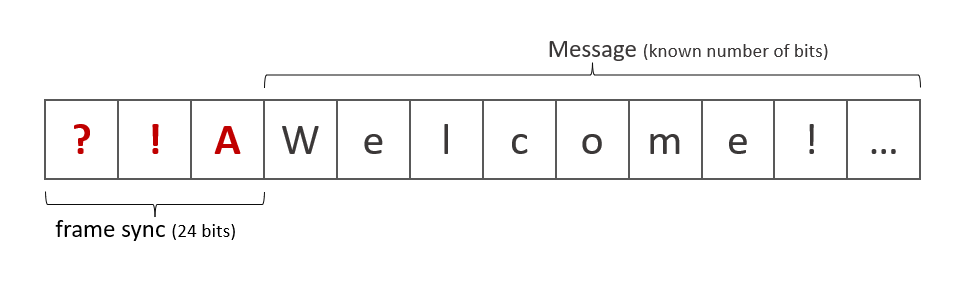
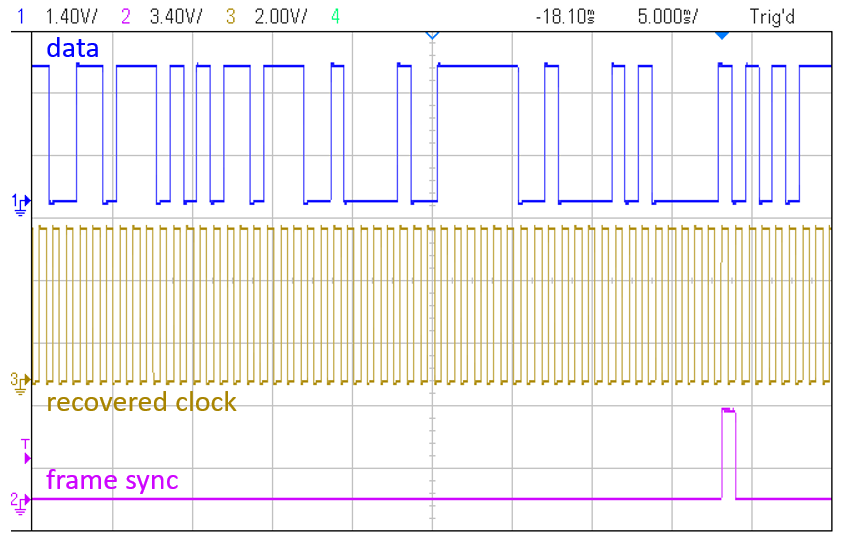
One thing that differentiate a real life implementation from the simulation presented here, is frame syncing. When simulating, the receiver always starts decoding the bitstream at the bit 0, without errors. But in a real system, even with the correct recovered clock, how the Rx will know when a new 8 bit character starts? And, how it knows if it started misaligned?
One practical solution is to append a known set of bits at the start of the message. The receiver first waits for locking of the clock recovery system and then, with correct timing, starts decoding the bitstream, bit by bit, as they arrive.
For each bit decoded, the Rx checks if it is the correct bit of the sync set. If it is the correct bit, it then waits for the next of the sequence. If it is not, it resets the checking, waits a new bit and starts to check from the first bit of the set again.
The receiver will only finish this checking step if all the sync bits are received in sequence, which signals that a full frame sync head was detected and the next bit will be the bit 0 of the message.
This technique guarantees synchronicity of the decoding. A new frame of data will be only valid if all the sync bits are received correctly again. In this project, I used three ASCII characters, ?!A, as sync, totalizing 24 bits.
AVR ATMega328 Implementation
For test purpose, I developed this full system running in a ATMega328, readily available in an Arduino Nano package. A pair of devices were used as Tx and Rx.
When implementing the Clock Recovery System in an environment with limited computing resources, like in real-time DSP, it is important to optimize the algorithm the maximum as possible. Fixed-point arithmetic is a must and, in the case of AVR ATMega architecture, the PI loop filter constants were applied using bit shifting.
Source Code
// Developed by Gregory F. Gusberti
// gusbertianalog.com
// youtube.com/allelectronicschannel

// NRZ Tx

const char *sync    = "?!A";
const char *message = "Welcome to gusbertianalog.com! Subscribe to All Electronics, open a beer a have fun!";

constexpr uint32_t BITRATE = 1200;
constexpr uint32_t Ts      = 1e6 / BITRATE - 2;

void setup()
{
	DDRB = (1 << 4) | (1 << 2);

	auto tx_nrz = [](const char *m)
	{
		uint8_t byte;

		while(byte = *m++)
		{
			while(byte)
			{
				PORTB = (byte & 0x80) ? (PORTB | (1 << 4)) : (PORTB & ~(1 << 4));
				byte  = byte << 1;
				_delay_us(Ts);
			}
		}
	};

	while(1)
	{
		PORTB ^= (1 << 2);
		tx_nrz(sync);
		tx_nrz(message);
	}
}

void loop()
{

}
// Developed by Gregory F. Gusberti
// gusbertianalog.com
// youtube.com/allelectronicschannel
// NRZ Rx - digital PLL Clock Recovery Loop
constexpr uint32_t OVERSAM = 32;
constexpr uint32_t BITRATE = 1200;
constexpr uint32_t Ts = 1e6 / (OVERSAM * BITRATE) - 4;
const char *sync = "?!A";
uint8_t sync_bitstream[24];
uint8_t sync_counter = 0;
constexpr uint16_t NCO_BIAS = (1l << 16) / OVERSAM;
static uint16_t PHASE_TARGET = 90 * (1l << 16) / 360;
static uint16_t nco_phase = 0;
static int16_t nco_word = 0;
constexpr int16_t Kp = 6; // bit shift division
constexpr int16_t Ki = 9; // bit shift division
static uint32_t integrator = 0;
static uint8_t nco = 0;
static uint8_t nco_last = 0;
static uint8_t input_register = 0;
#define _NOP() do { __asm__ __volatile__ ("nop\nnop\nnop\nnop\n"); } while (0)
void setup()
{
DDRB = (1 << 2) | (1 << 1) | (1 << 3);
for (int8_t i = 7; i >= 0; i--)
sync_bitstream[7 - i + 0] = (sync[0] & (1 << i)) != 0;
for (int8_t i = 7; i >= 0; i--)
sync_bitstream[7 - i + 8] = (sync[1] & (1 << i)) != 0;
for (int8_t i = 7; i >= 0; i--)
sync_bitstream[7 - i + 16] = (sync[2] & (1 << i)) != 0;
while(1)
{
if ((PINB & (1 << 4)) ^ input_register)
{
input_register = PINB & (1 << 4);
int32_t error = (int32_t)PHASE_TARGET - nco_phase;
integrator += error;
nco_word = (error >> Kp) + (integrator >> Ki);
}
else
{
// delay equalizer
_NOP(); _NOP(); _NOP(); _NOP(); _NOP(); _NOP(); _NOP(); _NOP(); _NOP();
}
nco_phase += nco_word;
nco_phase += NCO_BIAS;
nco = (nco_phase & (1 << 15)) != 0;
PORTB = (nco) ? (PORTB | (1 << 2)) : (PORTB & ~(1 << 2));
if (!nco_last && nco)
{
if ((0 != input_register) != sync_bitstream[sync_counter++])
sync_counter = 0;
if (sync_counter == 24)
{
PORTB ^= (1 << 3);
sync_counter = 0;
}
}
nco_last = nco;
_delay_us(Ts);
}
}
void loop()
{
}References
http://s53mv.s56g.net/dmostovi.pdf
https://en.wikipedia.org/wiki/Clock_recovery
https://download.tek.com/document/65W_26023_0_Letter.pdf
https://web.stanford.edu/class/archive/ee/ee371/ee371.1066/lectures/Old/Older/lect_17_CDR_2up.pdf
https://www.skylaneoptics.com/en/articles/clock-data-recovery-cdr/