Characterization of Crystal Resonators
This article explores the extraction of the electrical parameters of a crystal resonator. Crystals are the base component of high stability oscillators, an electronics sub-block that is essential for almost every electronic device of today's. The combination of low-cost, high precision and stability, low-power consumption and low phase-noise, made the crystal resonator the standard form for frequency generation.
Characterizing the device and extracting its parameters into an electrical model, enables the design of oscillators and filters using standard techniques. However, the measurements must be performed with attention, to truly capture the real behavior, something that is made difficult by the high Q nature of the crystal when resonating.
The electrical model must cover the characteristic frequency response of the crystal and its high (but not infinite Q). Two resonant regimes occur, near the frequency marked by the manufacturer, a series resonance and a parallel resonance.
Actually, one of the resonant regimes happens exactly at the marked frequency, but this will occur only if the crystal is utilized exactly as indicated by the manufacturer. For example, the manufacturer will specify the external capacitance that the oscillator will present to the crystal; the temperature; the voltage excursion; etc.
Crystals marked for series resonance will resonate at the specified frequency when all mentioned criteria are met, and the external oscillator circuit utilizes the series resonance. The circuit must be designed for utilizing the parallel resonance if the crystal is supplied for that.
However, having a proper model of the crystal allows the designer to utilize the crystal for different applications, as the behavior of the crystal is lumped into a capacitive and inductive sub-circuit. The addition of external inductances or capacitances around the crystal can shift the resonant-mode frequencies as needed (enabling, for example, the tuning of the oscillator's frequency).
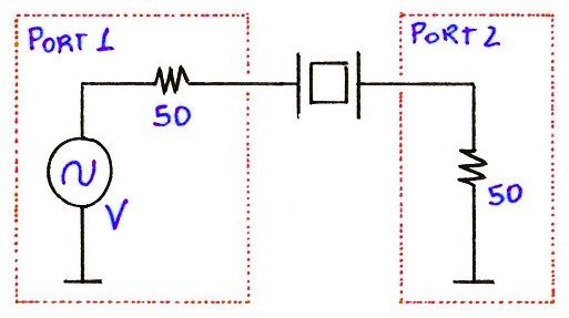
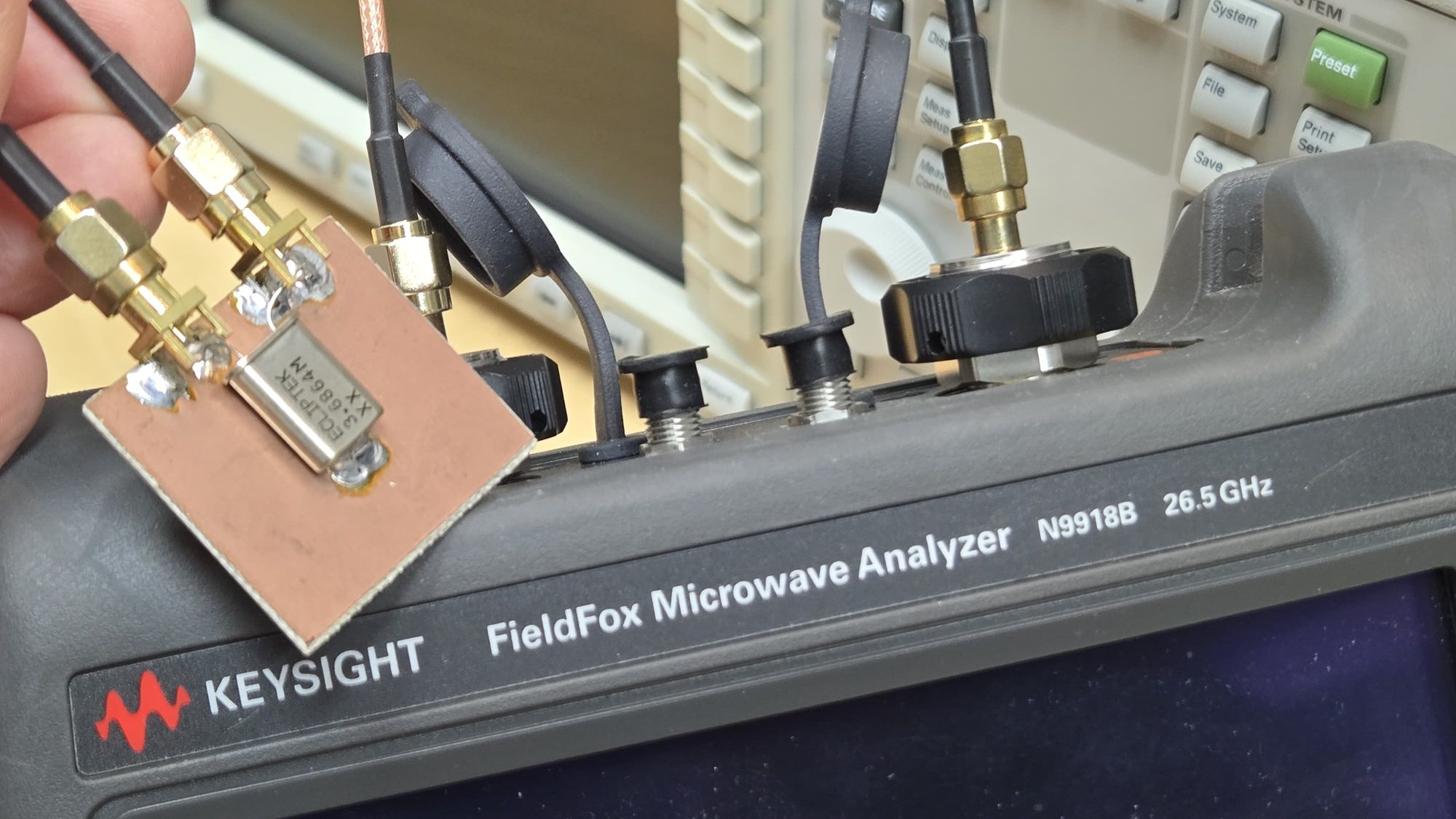
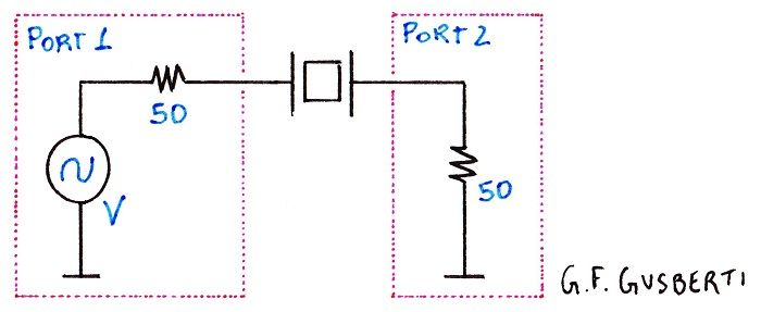
The crystal's behavior is analyzed by connecting it as a series element to the ports of the VNA. For this experiment, a Keysight N9918B FieldFox analyzer was used and, as the parameters are extracted using the S21 trace, any spectrum analyzer with tracking generator will serve the purpose. It is crucial to configure the equipment correctly, and more attention to this will be devoted at the end of the article.
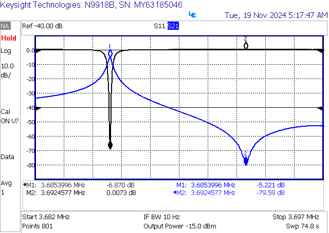
Figure 2 shows the two resonant regimes, an S11 trace is also active for the sake of the demonstration and will not be used for the characterization. Marker 1 is situated on the series resonance peak, and Marker 2 in the parallel resonance.
Series resonance means that the crystal presents a very low impedance at that frequency. The insertion loss of ~5.22 dB happens by the Equivalent Series Resistance (ESR) - that is, the electrical representation of the mechanical energy loss - responsible for the finite Q.
Parallel resonance occurs at a slightly higher frequency, in which the crystal presents a very high impedance. This mode happens as a side effect of the physical construction of the crystal, due to the shunt-capacitance introduced by the mechanical holder and electrodes [1].
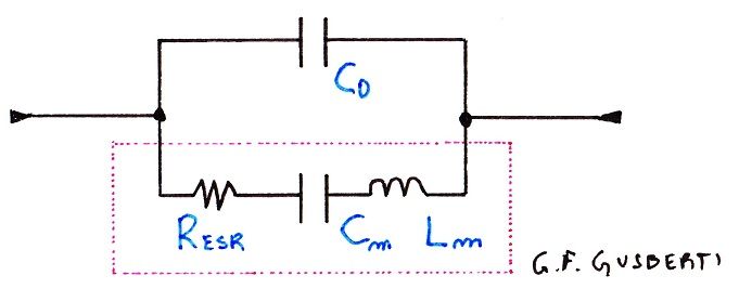
The electrical model consists of a series LCR resonator Lm, Cm, Resr, and a parallel shunt capacitance C0. Lm, Cm and Resr are the motional parameters, and are the electrical manifestation of the mechanical characteristics of the crystal cut. Lm models the vibrating mass, Cm models elasticity and, sometimes described as Rm, the Resr describes the mechanical loss [1].
By expanding the model, resonances that occur at overtone frequencies (odd harmonics of the fundamental) can be represented. This was explored here Overtone Crystal Oscillator, and it won't be discussed in detail in this article.
Lm and Cm are responsible for the series resonance directly, forming a series LC tank responsible for the low impedance behavior. The parallel resonance occurs through the parallel tank formed by Lm, Cm and C0 - notice that the motional inductance sees the series combination of both capacitances - thus always happening at a slightly higher frequency.
Observing that for parallel resonance, the capacitance seen by the motional inductance is the series combination Cp = Cm * C0 / (Cm + C0), the standard formula for tank resonance F = 1 / (2 * pi * sqrt(L * C)) can be applied simultaneously for both resonant regimes - considering that the parallel capacitance C0 is known - enabling the extraction of Lm, Cm.
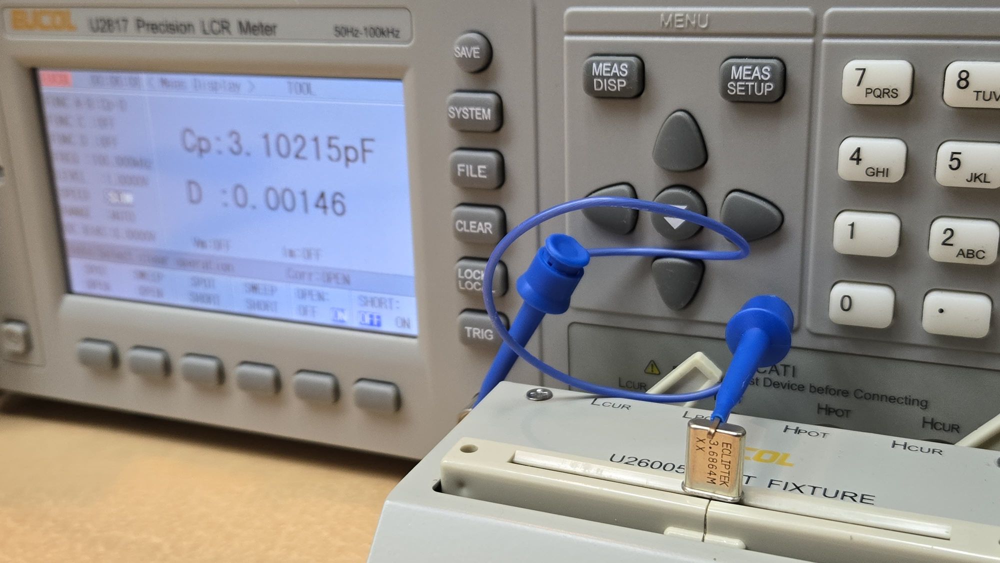
As the C0 capacitance is connected to both ports of the model, a direct determination of its value is possible using an LCR meter, as seen in Figure 4. Notice that the metal case of the crystal was grounded to the LCR's chassis, stabilizing the measurement.
For the last parameter required, Resr, the insertion-loss at the series-resonance can be used for the calculation, as at this frequency point the reactances of Lm and Cm cancel exactly and the series resistance is the only important component in the signal path (C0 is actually bypassing some of the series resistance current, but its effect can be neglect for the low Resr that usually is lower than ~100 Ohm).
The Resr is thus extracted by computing the voltage loss ratio in the analyzer Port 2, by the formed resistive divider, for the incoming wave arriving from Port 1. A voltage loss ratio 2 * 50 / (100 + Resr) - from the observation that for a perfect-through connection, the Port 1 excitation voltage is split equally between both port impedances - will lead to an S21 measure S21 = 20 * log10(100 / (100 + Resr)).

These final equations are then used to calculate the parameters from the measurement in Figure 2, leading to values Lm = 156.33 mH, Cm = 11.92 fF, Resr = 81.9 Ohm and C0 = 3.10 pF.
Quality factor Q can also be quantified by computing the ratio of energy stored in the big motional inductance Lm (through its reactance XLm) by the energy loss on Resr, thus Q = XLm / Resr leading to an enormous quality factor of about ~44200 for the tested crystal.
Crystal's Series and Parallel Resonance
When used in oscillators, one of the crystal's resonance regimes will be chosen. The fundamental method for achieving oscillation is different for each regime.
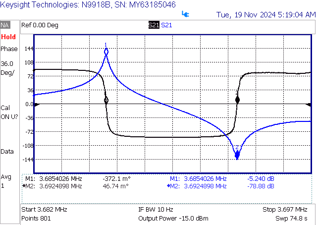
Adding an S21 phase-trace to the measurement allows for a better understanding of the behavior of the crystal for both resonant points. The crystal looks capacitive before reaching the series resonance (to the left of Marker 1). The phase crosses zero abruptly - due to the extreme Q - and the behavior switches to inductive (phase lead), this inductive region stays consistent in between the series and parallel resonances (Marker 1 to Marker 2, Figure 7).
By the frequency that the parallel resonance regime is met (Marker 2, Figure 7), the behavior switches rapidly again to capacitive, that is seen by the indication of a phase-lag in the phase-trace measurement. Above the parallel resonance, the C0 reactance starts to decrease, and it starts to bypass the current across the motional components of the crystal as the frequency increases.
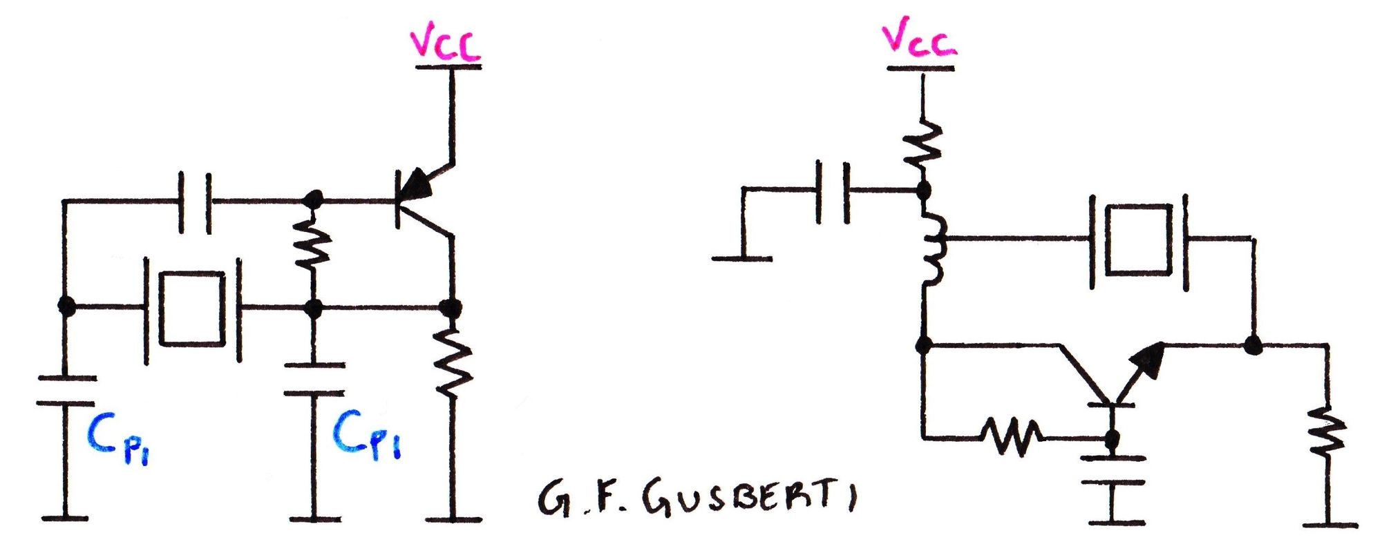
Figure 8 shows two oscillator topologies using the different regimes of resonance. On the right, the circuit utilizes the series resonance for closing the positive feedback loop directly, throwing part of the output power into the active element in phase.
The oscillator on the left - using a Colpitss-like topology - utilizes the inductive behavior in between resonant regimes (close to the parallel resonance), in combination with the shunt capacitors Cpi, to create the proper feedback phase for achieving oscillation. For this case, the crystal is serving as the inductive reactance of a pi LC network.
When using the crystal with any possible topology, the designer should also consider the loading capacitance presented to the crystal - this being the parasitic capacitance, external to the crystal, the circuit presents. This external capacitance will load the resonator and will appear in parallel with C0.
An adjustment to the equations is possible, replacing the C0 for the total capacitance seeing by the crystal - Ct - knowing that the total capacitance is the parallel combination of C0 with any other parasitic capacitance. For the case the external capacitance is called Ce, Ct = C0 + Ce and the calculations should be performed replacing C0 by Ct in every equation.
VNA Measurements of the Crystal
Measuring the crystal with the S21 trace as presented in the Figure 7 requires proper configuration of the VNA or the Spectrum Analyzer used. The extremely high Q factor of the crystal generates a very sharp resonance response, that will not show if the analyzer is sweeping too fast.
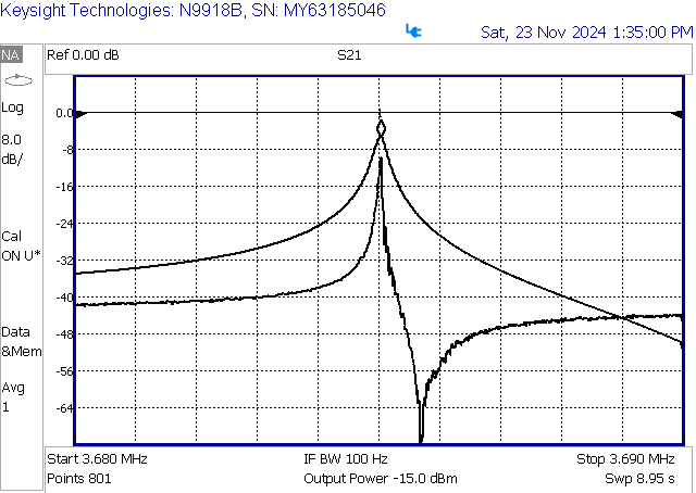
The parallel resonance regime requires a high signal-to-noise ratio, as the series impedance of the crystal will increase to large values, making the analyzer's trace wobble if the resolution bandwidth or IF bandwidth is not configured to a lower value than common.
To accurately capture the sharp series resonance peak (Marker 1, Figure7 or Marker 1, Figure 9), it is essential to reduce the sweep speed or increase the number of sweep points when using a lower IF bandwidth. Failing to do so may result in incorrect measurements of insertion loss, leading to an inaccurate calculation of Resr, as the resonance peak may not be displayed correctly.
Conclusion
For proper modeling and design of electronic circuits, it is crucial that good modeling of the parts is performed, with the application of the correct measurement techniques. With the model in hand, the engineer unlocks the ability to apply standard engineering methods to meet the required specifications.
By understanding the crystal as a combination of series and parallel resonances, it is possible to predict the effects of external reactances presented to the crystal, enabling the design of stable oscillators and filters, and adjustment of the center frequency (using trimmer capacitors or inductors).
Care should be taken during characterization, as the high Q of the crystal necessitates a non-standard configuration of VNA or Spectrum Analyzer. Failure to do so may result in an incorrect model. Accurate characterization ensures that the crystal's behavior is understood, providing a reliable foundation for optimizing circuit performance and achieving robust, predictable results.
Video: How to Characterize Crystal Parameters
References
[1] https://ecsxtal.com/124-quartz-crystal-design-parameters
