
5GHz Frequency Multiplier
Signal generators for microwave bands are expensive and difficult to obtain, especially over the L Band. This frequency multiplier, based on harmonic generation and filtering, works with low part count, easily extending the maximum frequencies at home labs.
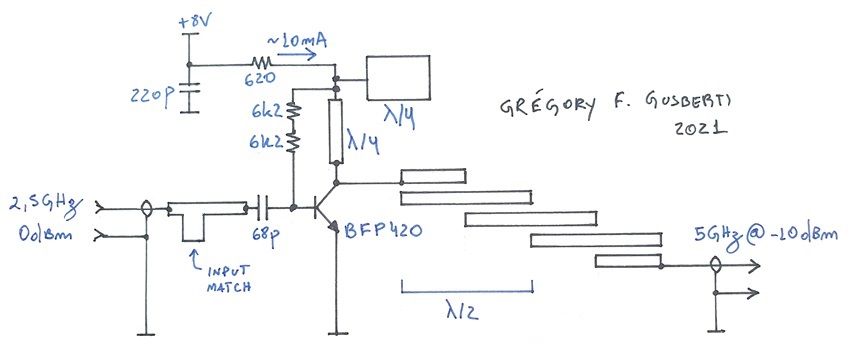
A modern BFP420 BJT is used as a saturated amplifier, producing strong harmonics of the input signal in its collector, thus the 2nd harmonic the desired output for frequency doubling. The input signal needs to excite the transistor over the P1dB. An input power of 0dBm achieves a good operation point and is a nice round value. Even so, higher input powers will generate higher output until full saturation of the 2nd harmonic power.
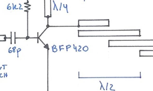
A lambda/4 bias tee easily bias the transistor, at the same time providing a high impedance for the output frequency. The DC operational point is configured by the 620R and 6k2 resistors. The two base resistors, in series, helps with isolation of the base RF energy and a microstrip printed inductor is recommended between them. If a different bias point is chosen, care need to be taken to ensure not exceeding the maximum very low collector voltage of the modern BFP420.
The fundamental and the not wanted harmonics are filtered out with the microstrip coupled-line bandpass filter. The overall construction, based on lambda/2 resonators and lambda/4 edge couplers, needs little or no tuning. Even so, if needed, small pieces of copper tape can be used to extend the length of the resonators.
The circuit works really well, even with no input match at all, generating a strong 5GHz @ -5dBm output signal. Slight higher output power was obtained with a rectangular piece of copper tape, working as a little open-end matching stub. The length and width were experimentally chosen to maximize output power (which does not necessary mean better input VSWR). The stub will probably have a length close to lambda/4, shorting the output frequency.
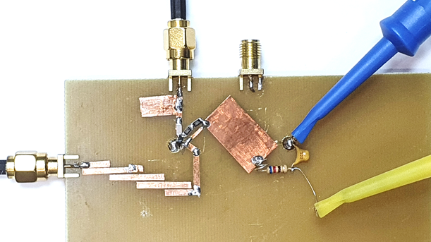
The prototype was made with copper tape on a single layer PCB of FR4 substrate. Even not being recommended for microwave work, FR4 helps, reducing the opportunity of self-oscillation of the transistor and of spurious resonant modes, because of the higher losses. Vias are made by drilling the PCB with a 3.5mm drill, closing the bottom-end with copper tape and filling the hole with solder, providing a good microwave GND connection.
The output filter coupling can be experimentally changed to achieve the best performance. As a rule of thumb, the resonators at the center are placed with looser coupling than the edge ones (higher physical separation, as seen in the picture). SMA connectors are used to bring the signals in and out of the board.
The construction with copper tape allows easy and fast prototyping of frequency multipliers of any frequency, being the output filter and the bias tee the main parts needing changes. Triplers and higher order designs follow the same principle of operation, although filtering the 3rd and even higher harmonics.
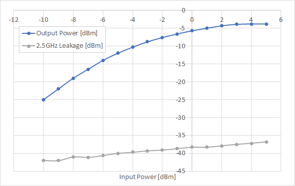
The relation of input excitation to output power shows that 0dBm is a good compromise between the maximum available output and the compression behavior. The output leakage of the 2.5GHz input signal shows itself at -33dBc (33dB lower than the main output tone), linearly increasing with higher inputs. It's interesting to note that, for the small-signal region of operation (until -6dBm input), the output tone grows two times faster than the input, because the 2nd harmonic originates from the squared term on the polynomial representation of the instantaneous collector voltage.
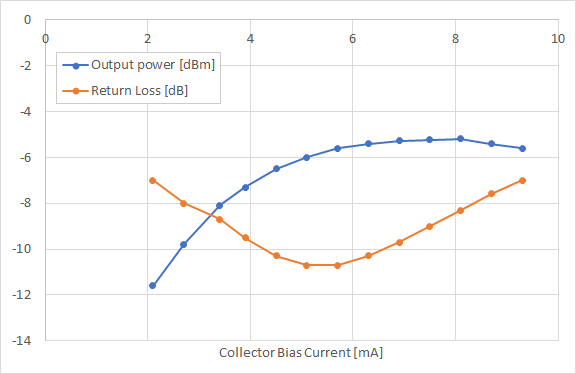
A sweep of the collector bias current shows the behavior of the input return loss and the output power. The fundamental non-linear principle of operation provides two different points for optimization. The best input match occurs near 5.5mA, which won't generate the higher output. Therefore, the bias point is a tread-off between different goals.
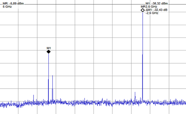
The output spectrum has an overall clean shape containing the 5GHz output and the input leakage, at 2.5GHz. Nevertheless, some spurious are present at uncorrelated multiplies of the input frequency, probably from parasitics modes of oscillation. A profounder investigation would help to understand the origin of the spurious signal, nevertheless, the low amplitude don't seem to be a concern.