Frequency Multiplier using CMOS gates

There are many ways to accomplish frequency multiplication in analog and digital circuits. In modern systems, PLL and DPLLs are the most common, allowing multiple frequency outputs with arbitrarily phase relationship.
Even so, a more fundamental approach, using harmonic generation, can be useful in a homebrew project, enabling fast prototyping, not requiring specialized knowledge. I demonstrated this concept in this YouTube Video.
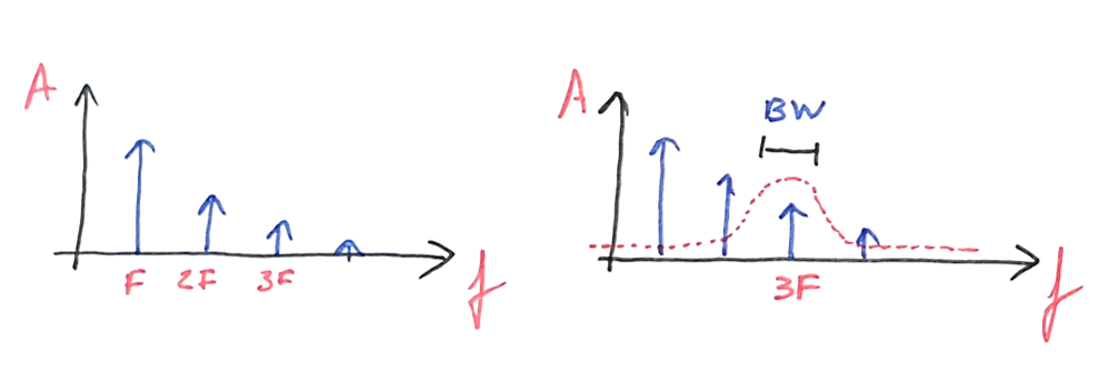
The idea consists in distorting a signal purposely, allowing the shift of energy from the fundamental input frequency to higher harmonics. The harmonic of interest (2x, 3x, 5x...) can now be filtered and amplified, giving at the output a signal multiplied in frequency and with steady phase relation.
Using a high gain amplifier stage, the input signal is distorted at the amplifiers output. In the simplistic example below, the square wave output of the inverter would be a good candidate for odd frequency outputs, because the symmetric square wave is rich in odd harmonics by nature.
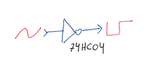
For small signals at the input, the NOT gate can be biased at the center point, operating as a high gain linear amplifier, you can learn more about this here.
The gate is self-biased by the feedback resistor at the center of equilibrium of the CMOS inverter stage, becoming meta-stable and very sensitive to input perturbations. Any small signal will swing the output of the amplifier high or low.

This output, now rich in harmonics of the input frequency, is filtered using a simple LC bandpass filter. The signal at the filter will contain higher power at the desired output frequency, but yet with a good amount at the sidebands (F - 1 and F + 1).
Cleaning the output is easy using additional gain stages. In this example, one more linear stage is used, amplifying the filtered signal almost to saturation. Full output saturation is guaranteed by the second output stage, providing the reduction of the energy at the signal sidebands.
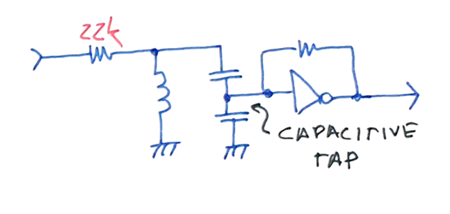
Smaller filtering bandwidth can be accomplished using a tapped resonator, allowing better selectivity of the desired harmonic. The tapping allows for impedance transformation of the output gain stage input impedance, as it dominates the impedance seem by the tank, lowering its effective Q.
You can also see that in the tapped resonator example, the feeding resistor was increased. This helps the increase of Q with a smaller drop of signal swing, because the low input impedance of the following stage is transformed by the C tap.
Multiplier for 107.2MHz - update: 02/02/2022
I recently designed a Microwave 10GHz Signal Source where the reference source needed to be a low phase-noise ~107.2MHz signal. My initial idea was to use a 5th Overtone Crystal Oscillator, using a 21.44MHz crystal. The crystal I got had very poor performance at the 5th harmonic, so I decide to run the oscillator at its main frequency, with a 5x multiplier at its output.
The multiplier designed uses CMOS gates from the 74AC series, running well at the ~107MHz output. The 74AC series also presents very clean and fast rise/fall times, needed for the subsequent modules of the project.
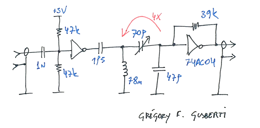
The input signal is AC coupled to the first amplifier, using a voltage divider at its input for bias around the center point. Lately, I'm preferring to use this fixed bias approach instead of the self-biasing as I used in the second amplifier, it works fine and present no risk of oscillation.
The output of the first amplifier, rich in higher frequency harmonics, is AC coupled to the bandpass filter using a very low value capacitor. The 1p5 capacitor presents a 1k ohms reactance at the output frequency, allowing very high loaded Q in the resonant structure.
The inductor was the only available in the lab, with ~80nH the reactance at resonance is ~50 ohms, much lower in comparison with 1k, shunting strongly the harmonics out of the 5th harmonic band.
The capacitors of the tank are split in two, one variable for adjustment. The capacitive tap helps with an impedance transformation of 4x, reducing the load in the tank. When calculating the capacitances, you need to consider that the gate input will add ~5pF to the bottom capacitor.
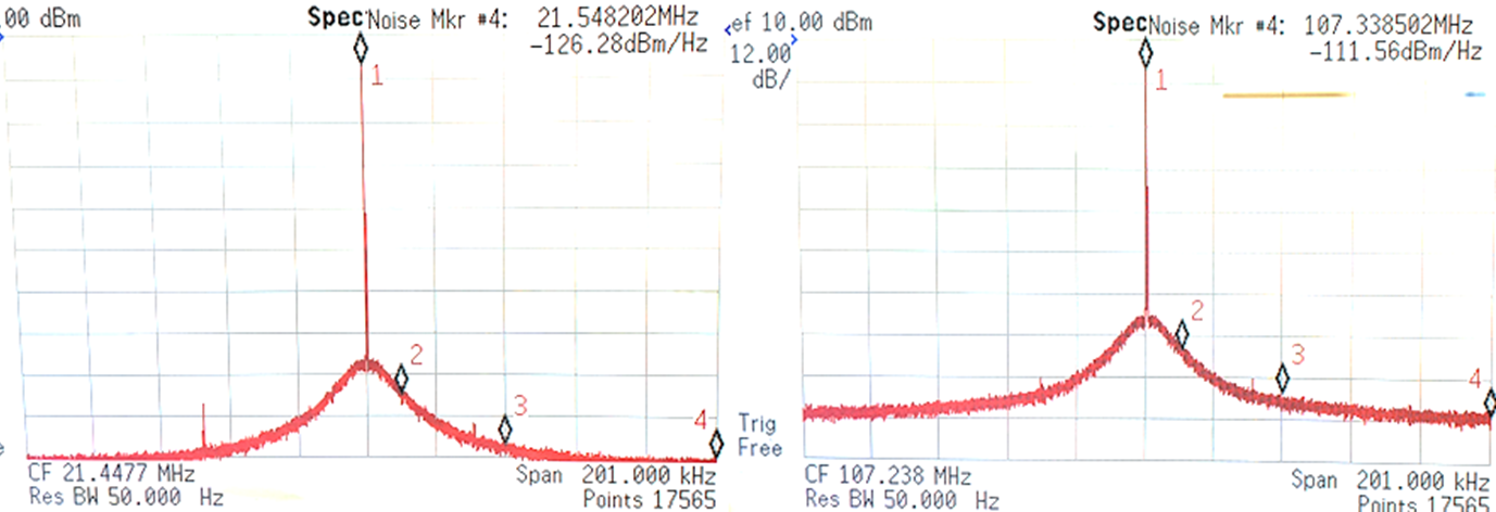
Phase noise at the output is right on the predicted theoretical degradation of 20 * log(N), where in this case N = 5. The input phase noise is limited by the signal generator used.


I also tested the multiplier running at 3V5 supply, the results seems the same.

These results show us that the phase noise degradation, by noise added from the circuit, is at least 10dB lower than the theoretical degradation, as no effects were detected with the measuring setup available at the lab. A cleaner signal source and a proper Phase Noise Analyzer would help with the full characterization of the architecture, showing the real noise floor available from this circuit.
