
Effective Methods for Dielectric Constant Characterization in PCB Design
This article explores three methods for determining the effective dielectric-constant of a PCB material. These techniques allow the extraction of the effective-permittivity for a given microstrip geometry, and the estimation of material permittivity for use in simulations and circuit design.
Relying on a practical measurement of the PCB, as the first step of a new design, permits speeding up the engineering phase, achieving the expected results when dealing with low-volume prototypes.
The three methods discussed in this article are: Ring Resonator, Delta Line Pair and Time-Interval for Impedance-Discontinuity Pair.
The characterizations rely on measuring frequency and phase resonant-points, or reflection peaks in the time-domain. By arranging equations that compare the measurements to ideal calculations, the effective permittivity 𝛆e and PCB material relative permittivity 𝛆r can be found.
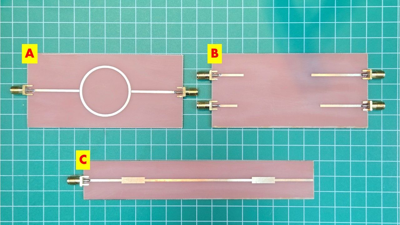
Figure 1 depicts the sample PCBs manufactured for the application of the characterization methods. These are made with 0.8 mm thickness FR4, the same material intended in the final design (where the PCB material will be used), and were fabricated with DIY methods.
The sample A is a ring resonator with two feeding probes going to the SMA connectors. Sample B presents two pairs of lines, with a length difference (delta) between the lines of each pair. Sample C uses a single transmission line with two impedance discontinuities at a precise separation.
Ring Resonator
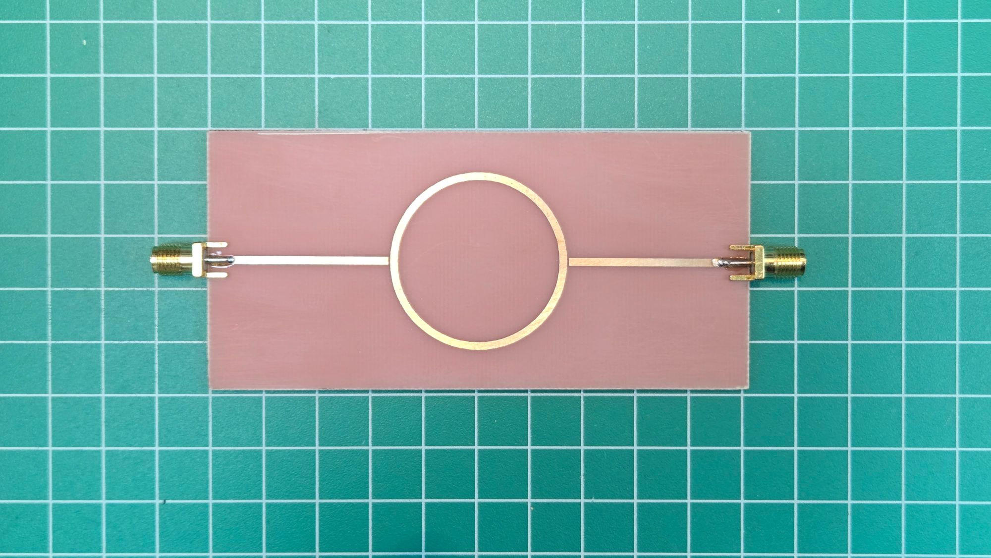
The ring resonator can be seen in Figure 2. It consists of a circular microstrip closed-path centered on the board. Two feed-lines couple the signal to the SMA connectors, with a coupling gap of ~0.3 mm. The precise circumference length of 100 mm dictates its resonant properties.
All microstrip features are made with the same width of 1.5 mm, that gives an approximate 50 Ohm impedance for the 0.8 mm FR4. As the exact dielectric constant of the material is yet unknown (and a precise impedance is not required), a ballpark value of 4.5, common for FR4, was used for calculating the trace width using [1].

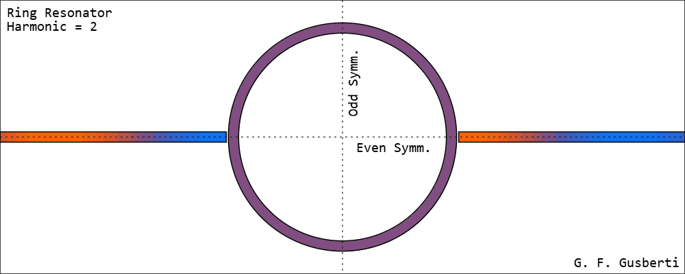
A Ring Resonator resonates at integer multiples of its effective length [2]. Field amplitudes are demonstrated in Figure 3.
Energy reaching the end of one feed-line couples to the ring and flows to both of its sides simultaneously - meaning that the ring can be divided with a horizontal line of even symmetry. Thus, the standing-wave pattern presents two voltage nodes situated at the odd symmetry line, as the traveled distance to each node is λ/4.
It becomes clear that the ring is resonating at full-wave, as the opposite side - at the second feed-line - will present a voltage anti-node with opposite polarity. The same anti-node pattern, with opposite voltages at both feed-lines, exists for any integer multiple of λ.
If an S21 measurement is performed across both ports of the rig, we expect transmission peaks for every integer resonant mode. The coupling factor must be low - coupling is inversely proportional to the feed-line gap - to reduce the resonator loading as much as possible.
The low coupling ensures that the S21 measurement closely approximates the unloaded Q of the resonator, minimizing frequency shifts due to loading and enabling the extraction of the material loss-tangent. I recommend adjusting the gaps to maintain the transmission peaks below -35 dB.
Using the speed of light as 3 × 10⁸ m/s, the resonant frequency Fn for a full-wave resonator of length L, resonating at the harmonic n is given by:
$$\tag{1} F_n = \frac{3 \times 10^8 \times n}{L \times \sqrt{e_e}}$$
The constant 𝛆e is the effective permittivity (or effective dielectric constant) for the specific geometry of the microstrip line and the PCB dimensions, and it is always lower than the PCB material 𝛆r. The difference arises due to the electric-fields being not entirely immersed in the PCB substrate, with part traveling in the air [3].
As the effective permittivity is what the electromagnetic wave sees, it is the practical constant factor by which the speed of light is reduced. Analysis done on the measurements will actually arrive at 𝛆e, and the material 𝛆r can then be estimated by back-calculations based on the microstrip width and PCB substrate height [4].
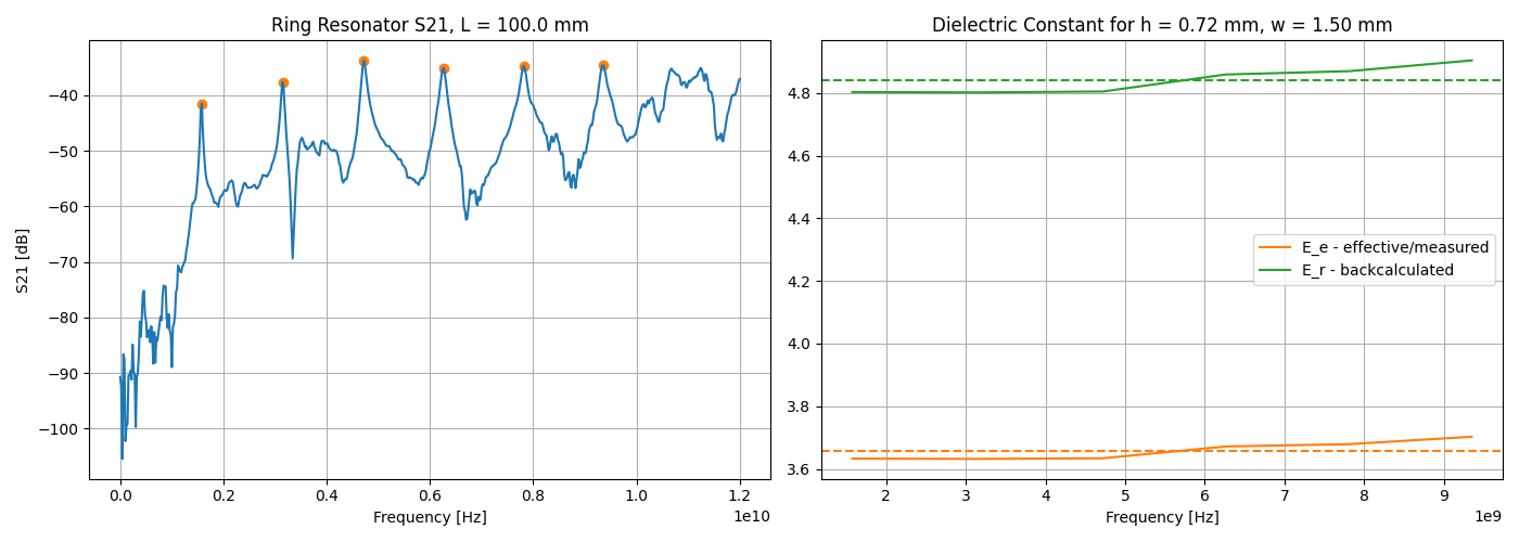
A transmission measurement was performed using a Keysight FieldFox N9918B VNA, and the trace data captured for further analysis. As seen in Figure 5 (left), the frequency-periodic peaks occur at every resonant mode of the ring, and the S21 measures below -35 dB for any of them.
By using a script to detect the peaks, the effective permittivity can be calculated for every resonant frequency, using (1) in reverse, leading to the orange trace in Figure 5 (right). The calculate values are stable over frequency and show a small increase for higher frequencies, behavior also noted in other sources [5]. The dotted orange-line shows the average of all measurements, at a value of 3.65.
When applying (1), the peak-frequencies captured may not represent exactly the resonant point, owning to the fact that the VNA measurement is discrete in frequency due to is working method. A better estimation of the peak frequency can be accomplished by fitting a parabola to every peak, using the S21 samples immediately to its left and immediately to its right. This technique is explained in detail in [6] and was used for the calculations.
$$\tag{2}e_e = \frac{e_r + 1}{2} + \frac{e_r - 1}{2} \times \left(1 + \frac{12 \times H}{W}\right)^{-1/2}$$
Equation (2) is commonly used to determine the effective dielectric for a specific microstrip geometry - where H is the height of the substrate and W is the width of the line - and the material's 𝛆r is given [6]. This equation was concepted by curve-fitting, and it works well for general use where accuracy of 1% or better is required.
$$\tag{3}a = \frac{1}{\sqrt{1 + 12 \times (H/W)}}$$
$$\tag{4}e_r = \frac{2 \times e_e + a - 1}{1 + a}$$
By applying (2) in reverse, we can solve for the substrate permittivity 𝛆r using the effective permittivity calculated over the measured data and the dimensions used for the construction of the ring resonator, with (3) and (4). The results are shown with the green trace on Figure 5 (right), where the dotted line displays the average of 4.84.
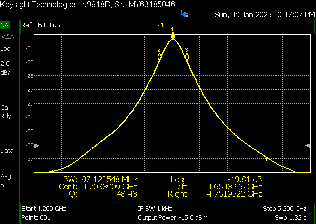
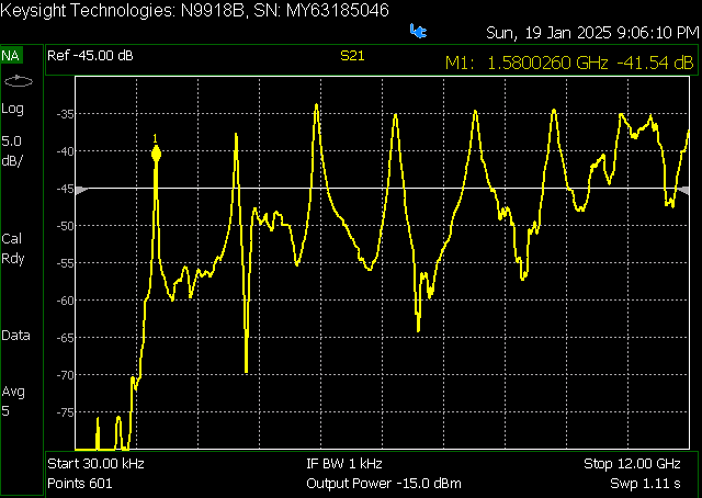
An advantage of the ring-resonator method is that it allows the measurement of the substrate loss-tangent, using the -3 dB bandwidth of the resonant peaks. Figure 6 shows a measurement done directly on the VNA, where the measured Q factor of ~50 agrees with a loss-tangent of 0.02 as commonly considered for FR4.
Delta Line Pair
One can imagine that the effective permittivity could be extracted by measuring the resonance of a single microstrip stub, he would not be totally wrong. However, the setup would suffer from two major parasitic effects: fringe capacitance and the SMA coaxial-to-microstrip transition.
The fringe capacitance arises due to the fringe fields because the electromagnetic field do not end abruptly at the end of the line [7], increasing a bit the electrical length of the resonator. On the feed side, the SMA connector also adds electrical length and complex resonances, due to the hard transition between propagation modes and the physical dimensions.
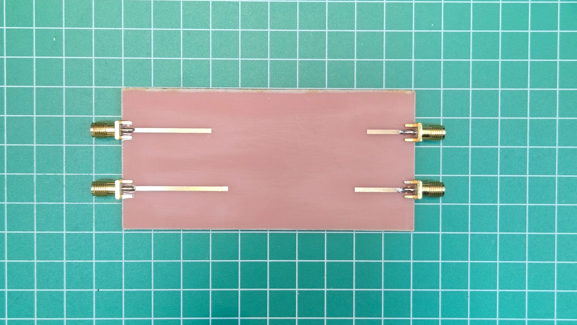
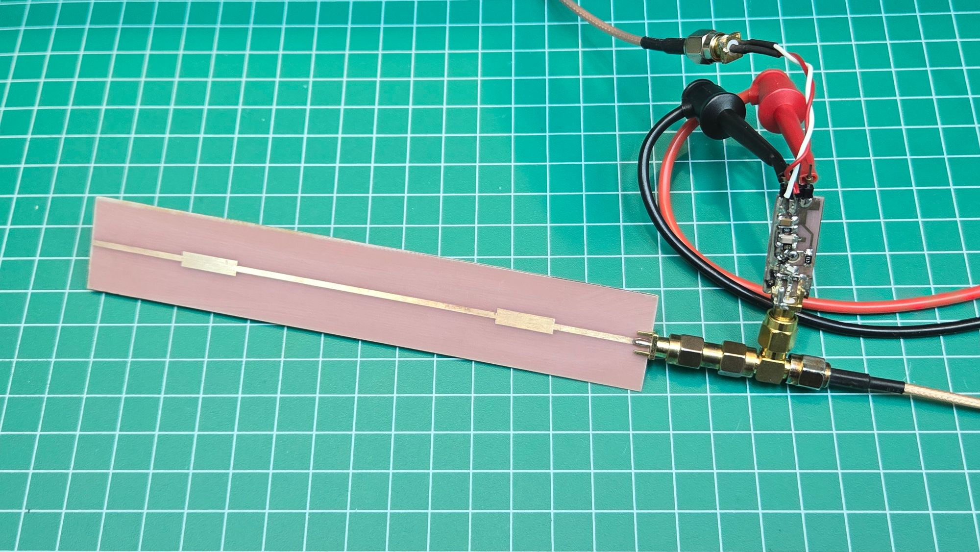
A pair of lines can be used to compensate for these effects, where a precise difference in length (delta) is used as the physical parameter for the calculations. As the electrical length added by the SMA connector and the fringe effects are similar in both resonators of the pair, they tend to cancel out. Figure 7 shows the test PCB, with two pairs: pair A lines having 30 and 36 mm, and pair B having 16 and 20 mm.
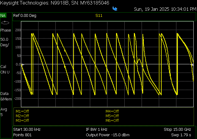
One way of measuring the resonance of a stub - or other microwave structure - with precision is by looking at the phase-response of the S11 measurement. For a theoretical stub, that does not radiate power, the S11 magnitude will be constant at 0 dB (as all power is reflected), but the phase will show exactly the resonance behavior.
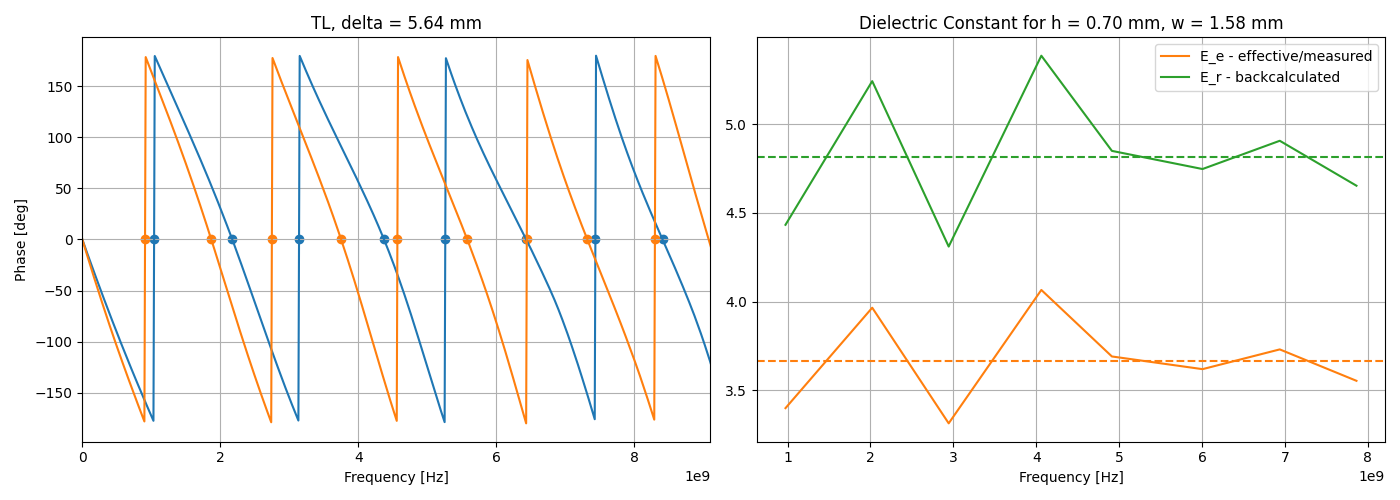
Figure 8 shows the phase response measured for a pair of stubs. The periodic behavior happens by the nature of the standing-wave, where the phase crosses 0 degrees every λ/4, at the specific frequencies where the stub looks like a short or open circuit. The length difference (delta) between the stubs makes the phase response to shift in frequency, where the 0 degrees frequencies are further apart for higher resonant harmonics.
$$\tag{5}F^1_n = \frac{3 \times 10^8 \times n}{4 \times L \times \sqrt{e_e}}$$
$$\tag{6}F^2_n = \frac{3 \times 10^8 \times n}{4 \times (L + d) \times \sqrt{e_e}}$$
$$\tag{7}e_e = \left[\frac{3 \times 10^8 \times n}{4 \times d} \times \left(\frac{1}{F^1_n} - \frac{1}{F^2_n}\right)\right]^2$$
Equation (5) gives the resonant frequency for a microstrip stub of length L, at the standing-wave harmonic n (multiple of λ/4). Considering a pair of resonant lines with a length delta d, we arrive at equation (6), that is equal to (5) but with the increment in length added to L. Frequencies Fn come directly from the measurement of both lines, and correspond to the zero crosses of the phase (every frequency where the stub resonates at multiples of λ/4).
By solving for the effective permittivity 𝛆e, using the known delta-length d and measured frequencies, we arrive at equation (7). The major error term introduced by this method is from the determination of the length difference, as the equation depends on its precise absolute value. The frequencies are not of big concern, as any modern VNA will measure it with precision to many decimal places (considering the setup is stable).
A script can be used to capture all zero crosses of the phase measurement from both lines in the pair, and the effective permittivity calculated automatically. The material permittivity is thus estimated by equations (3) and (4). The delta length used was measured from the manufactured PCB, to accommodate any fabrication error.
Interpolation was used to determine the zero-crosses, similarly as how it was done for the Ring Resonator method. For the phase, as it changes linearly, a simple line fit was performed with the frequencies immediately before each zero-cross and immediately after each zero cross, with the 0 degrees frequencies used in the calculations being back calculated from the fitted line segment.
Figure 9 depicts the results. At the left, the phase profiles of both lines in a pair and its zero-crosses are shown. At the right, the effective and relative permittivity are displayed. The results are much less stable when compared to the ring resonator method, with a large variance for lower frequencies.
Both dotted lines show the average of the permittivity. Considering that this averaged result represents better the real value, we arrive at an effective permittivity of 3.66, and a relative permittivity of 4.82 for this method.
The variance may happen by the sensitivity of the method, relying on the delta-length d as the absolute physical parameter. Besides that, the cancelation of the electrical length added by the SMA connector and the coaxial-to-microstrip transition is not perfect.
Time-Interval for Impedance Discontinuity Pair
Both methods presented before are what we call frequency-domain methods because the measurements performed with the VNA are based on exciting the DUT at different frequencies, where the required S parameters are computed. However, measurement in the time-domain can also be accomplished, leading to similar results.
The idea of exciting a microwave structure and measuring its response in time is old and is mainly known as TDR - Time Domain Reflectometry, and it consists in generating a very fast pulse - in the picosecond range - that travels through the DUT [9]. As the pulse wavefront encounters impedance discontinuities, part of the energy is reflected and these reflections are displayed using an oscilloscope.
When comparing with a frequency-domain method, every measurement parameter is reciprocal due to the frequency-time duality - a higher bandwidth measurement means a shorter pulse in time. Frequency-domain characteristics as the S-parameters become time-domain T(DR)-parameters T11, T21, etc. [10] (not to be confused with Scattering Transfer Parameters, also called T-parameters).
The effective permittivity can be extracted by measuring two reflections happening at known positions in the fixture, for the arrival time of these reflections will be directly related to the propagation velocity of the microstrip geometry.
Figure 11 shows the behavior of the fixture used for the test, where the two small segments of lower impedance are placed at a known distance. The pulse starts propagating into the structure from the left, advancing to the right as the time passes. The key observation is that, by assuming a non-dispersive medium, time is directly proportional to position in space.
As the wavefront encounters the first impedance discontinuity (point A), part of the energy is reflected as a negative voltage pulse - due to the transition from a higher to a lower impedance. The main pulse keeps traveling on the structure and meets point B - where a transition from lower to a higher impedance occurs - generating a new reflection, now with positive voltage.
The same occurs for every discontinuity, with reflect energy propagating back to the input port. By attaching an oscilloscope to the input port, in parallel with the pulse source, the sequence of reflections can be observed in the time-domain (this is the T(DR)11 trace, the time-domain dual of the S11 trace).
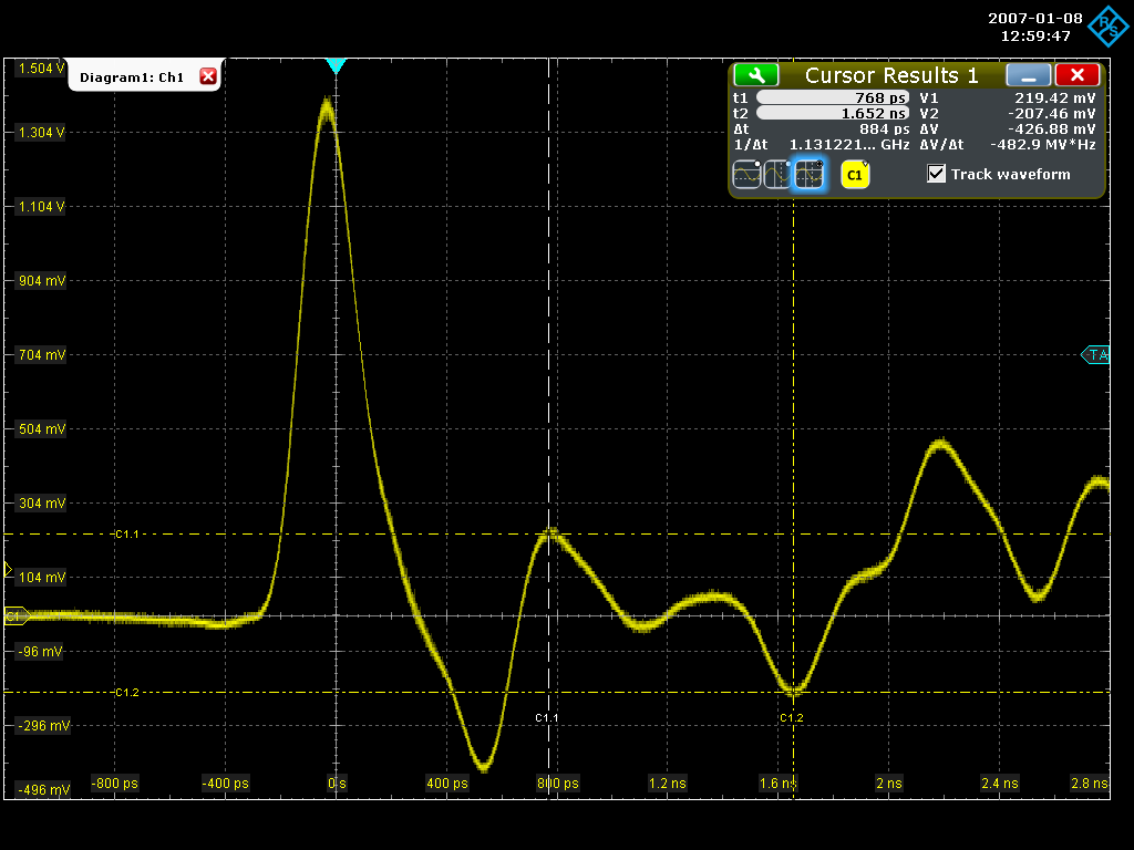
Figure 12 depicts the reflection profile measured for the test PCB. The first (and strongest) pulse is the excitation generated by the pulse source, with a Gaussian-like shape and a width of ~220 ps. Every pulse that follows corresponds to one of the physical reflection points, where the positive or negative amplitude prints the discontinuity type - higher to lower or lower to higher impedance.
$$\tag{8}\delta S = \frac{3 \times 10^8 \times \delta t}{\sqrt{e_e}}$$
$$\tag{9} e_e = \left(\frac{3 \times 10^8 \times \delta t}{2 \times \delta S}\right)^2$$
For a microstrip geometry with effective permittivity 𝛆e, the distance length δS propagated by the wavefront is given by equation (8), where δt is the propagation time. By rearranging for 𝛆e, and considering the delta-time between reflections, we arrive at equation (9). The physical distance between the reflections must be multiplied by two because the time difference measures the round-trip time of the signal.
The final assembly presented a distance of 139 mm between point B and point C, in oppose to the 140 mm used in design, showing the importance of measuring prototype PCBs before any calculation is performed. Using a time-marker on the oscilloscope, the delta time between the reflections was measured as 884 ps, that results in an effective-dielectric of 3.64 by the usage of (9).
Generation of the fast pulse was accomplished by a BJT transistor working in avalanche, where the energy stored in a capacitor is dumped on the 50 Ohm output. The details of this circuit will be addressed in a future article. Different ways of connecting the pulse-generator + oscilloscope + PCB were tested, as power splitters, directional couplers and resistive combiners, with the best results generated by the simple SMA T-connector.
Conclusion
This article explored three different methods that are successful when accomplishing the measurement of the effective and relative permittivity of a given PCB material. By starting with the most common and stable method, the Ring Resonator, a baseline for the other two setups was set. The table below summarizes the results.
| Method | Effective Permittivity | Relative Permittivity | Loss-Tangent |
|---|---|---|---|
| A. Ring | 3.66 | 4.84 | 0.20 |
| B. Delta-Pair | 3.65 | 4.83 | N/A |
| C. Time Interval | 3.64 | 4.81 | N/A |
| Average | 3.65 | 4.83 | N/A |
For the extraction of the loss-tangent, the ring is the only method that can perform it. The automated scripts used for detecting the peaks and calculating the permittivity could be easily enhanced for the calculation of Q and loss-tangent for each peak.
The Delta-Line pair showed a large variance, primarily at the lower test frequencies, where the sensitivity of the equation is higher due to smaller difference in the phase response profile. Nevertheless, the mean result agrees with the ring resonator with less than 0.5% of divergence.
Demonstrating a measurement in the time-domain expands the reader's toolbox, showing that the TDR method is viable without expensive equipment, for the usage of a homemade picosecond pulser. However, the high-bandwidth oscilloscope is still required and its replacement by a DIY device is open for further exploration.
The determination of the reflections pulse timing is tricky when done by hand, where wrong positioning of the markers will offset the delta-time reading by a significant amount. Even so, the calculated effective permittivity agrees with the ring resonator by less than 1%.
Characterization a PCB substrate dielectric is crucial for microwave design and for achieving proper results with the least amount of trial-and-error iterations and, by the end of the article, the reader should be able to perform the chosen method without requiring time-demanding simulations or complex calculations.
References
[1]⠀https://www.allaboutcircuits.com/tools/microstrip-impedance-calculator/
[2]⠀https://www.circuitinsight.com/uploads/2/measuring_impact_test_methods_high_frequency_circuit_materials_smta.pdf
[3]⠀https://www.microwaves101.com/encyclopedias/microstrip
[4]⠀https://www.signalintegrityjournal.com/articles/2378-measuring-the-bulk-dielectric-constant-dk-on-a-microstrip-with-a-tdr
[5]⠀https://ieeexplore.ieee.org/document/1650455
[6]⠀https://cds.cern.ch/record/720344/files/ab-note-2004-021.pdf
[7]⠀https://www.microwaves101.com/encyclopedias/microstrip
[8]⠀https://www.ntuemc.tw/upload/file/2011021716275842131.pdf
[9]⠀https://www.keysight.com/br/pt/assets/7018-01179/application-notes-archived/5988-9826.pdf?success=true
[10]⠀https://download.tek.com/document/TVMP-0404.pdf