
Why impedance matching still matters for transistors
This article aims to explain why impedance matching is required for extracting the maximum gain from transistors, as is typically required in RF applications. We start by using a rough model of the transistor's input and then perform a full small-signal analysis, proving the argument in depth.
Transistors are usually thought of as very high-impedance devices, leading to the premature conclusion that they work as voltage sensors and that directly connecting them to a low-impedance source yields maximum performance.
While voltage bridging is standard for audio and broadband circuits, it becomes a bottleneck in RF design, where the priority shifts from voltage fidelity to power efficiency and noise-figure optimization (noise matching is a separate optimization and is beyond the scope of this article).
Figure 1 shows a signal source modeled by its Thévenin equivalent and a BJT amplifier in the common-emitter configuration. The transistor is drawn just for the sake of clarity, with the coupling and biasing circuitry omitted.
The 1 kΩ resistor models the AC small-signal input impedance of the BJT amplifier and can be thought of as the base (or base-emitter for grounded-emitter configurations) differential impedance as seen from the base, for the sake of this example.
$$\tag{1} U_{b} = 0.2\,\frac{1000}{100 + 1000} = 181\,mV_{rms}$$
Equation 1 shows that the excitation at the base of the transistor in Figure 1 will be 181 mVrms, calculated as a simple voltage divider. Since the amplifier input impedance is ten times higher than the source's, the generator's voltage swing transfers almost perfectly to the base.
This model works well at low frequencies but breaks down when the goal shifts from voltage transfer to power efficiency, which is precisely the situation in RF design.
We now change perspective and start to look at the problem from the angle of the power delivered to the transistor amplifier.
It is possible to calculate the available source power (Pavs) that the source can deliver by considering its connection to a matched load, as seen on the left side of Figure 2.
$$\tag{2}\begin{aligned} U_{avs} &= 0.2,\frac{100}{100 + 100}{} = 100\,mV_{rms} \\ P_{avs} &= \frac{U_{avs}^2}{100} = 100\,uW \\ P_{b} &= \frac{U_{b}^2}{1000} \approx 33\,uW \end{aligned}$$
The power delivered to the transistor base, Pb, is a fraction of the maximum available power, Pavs.
Thus, it should be clear that if more power were to be delivered to the transistor, the excitation voltage on the base would be greater, as the AC small-signal input resistance follows Ohm's Law: Pb is proportional to Ub2 / Rb, where Rb is the resistive part of Zb.
A larger Ub swing will always be a direct result of a higher delivered power. In other words, since the input resistance is fixed for a given bias point, the only way to physically increase the voltage across it is to pump more power into it.
Figure 3 shows the configuration with an impedance matching network added between the signal source and the transistor amplifier. The matching network bridges both impedance profiles: the generator side working at 100 Ω and the amplifier side working at 1 kΩ.
Presented with a 100 Ω load, the generator can deliver all its available power to the input port of the matching network. Then, by increasing the voltage at its output port, the matching network excites the transistor at a higher level than in the voltage bridging scenario, delivering all the incoming power from the source.
The transistor now sees a higher excitation voltage at the base, leading to a stronger electric field in its base-emitter junction. From that follows a greater modulation of the collector current that generates a higher output.
It is key to understand - and that comes from adopting the RF perspective - that the fundamental limit is the power the signal source has available to deliver. In principle, no theoretical limit exists for voltage or current ratios in a lossless network, and the same amount of power can be represented by different ratios of voltage and current.
Specifying impedance is equivalent to specifying the voltage-to-current ratio: the signal source presents 100 Ω and the transistor input presents 1 kΩ. The matching network thus has the task of converting between these ratios: increasing the voltage by the square root of the impedance ratio, allowing the delivery of all the source's available power to the transistor.
The 1 kΩ resistor in our simplified example was chosen to clearly illustrate the power transfer argument. While this ideal lumped-resistor model demonstrates the concept of power transfer, real transistors have internal parasitics that make the input impedance complex and frequency-dependent.
To see how this works in practice, we must look inside the silicon.
Transistor Small-Signal Model
In the first part of the article, we represented the transistor as a single 1 kΩ resistor and treated the voltage across it as representative of the transistor's base voltage. Now, we proceed with a small-signal analysis of a practical transistor circuit, including the junction capacitances and additional parasitics.
A practical transistor amplifier is shown in Figure 4. The transistor is biased at 10 mA by Rbias and the 100 R resistor, forming a stabilized biasing network: an increase in the DC collector current leads to a greater voltage drop across the 100 R resistor, resulting in a lower current into the base (that steers the operating point back to equilibrium).
In the example, the output load ZL is resistive and is represented by the 200 R resistor. The resistance RE is used to improve linearity, and any excitation provided by the base voltage swing will be divided between it and the transistor's base-emitter terminals.
Now, let's navigate the world of small-signal modelling.
The small-signal model is a linear model that mimics the AC behavior of the transistor for small perturbations over a given bias condition. The model is key for understanding the behavior of the transistor at high frequencies because it allows direct application of linear tools (like frequency response analysis and Laplace transforms).
The reader should internalize the concept that the small-signal model represents the transistor for that specific bias condition. It linearizes the behavior of the transistor at the quiescent point and is valid for signals that are not large enough to excite the non-linearities.
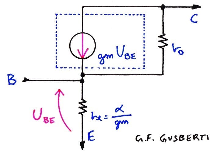
Figure 5 shows the starting point for the small-signal model. The T-model is composed mainly of the re resistance, the dependent current source, and the output resistance ro. The resistor re models the dynamic resistance of the base-emitter junction and is directly excited by Ube, the resistor ro models the Early Effect, and alpha is the emitter-to-collector current transfer ratio.
The current source models the behavior of the transistor's collector and is controlled by Ube and the transconductance gm. For a given bias point - meaning a fixed gm - maximizing the voltage swing over the base-emitter dynamic resistance re will maximize the current swing at the collector.
It is possible to expand the model by adding the junction capacitances and the base spreading resistance rb. Cbe (also called Cπ) models the base-emitter junction and diffusion capacitances, and Ccb (also called Cμ) models the base-collector junction capacitance. More complex models can include a collector-emitter capacitance, Cce, which is not used in this article.
A further enhancement of the model is made by adding the bulk resistances of the silicon + metal connections for each port, usually named rbx, rcx, and rex, and package inductances LB, LC, and LE.
The model used in the article is shown in Figure 6 and ignores the emitter and collector bulk resistances and inductances (rex, rcx, LE, and LC). The base spread resistance rb and inductance LB are kept in the model and appear before the resistance re, those are kept to emphasize the argument made in the article.
At the output of the model, the inclusion of ZL models the impedance of the load connected to the collector of the transistor, and C0 models any output stray capacitance.
The biasing components are not included in the model for this example because their values won't impact the analysis (the Rbias at 72 kΩ is very high, and the coupling capacitors and choke inductor are a short and open circuit, respectively).
Modulation of the collector current - that produces an output voltage swing over ZL - continues to be determined by the voltage across re but, as it is clear in Figure 6, this voltage is now internal to the transistor model and is named Uj (junction voltage) to differentiate it from the terminals' voltage Ube.
Also, in Figure 6, it is possible to see the addition of the resistance Red, which is not part of the transistor model itself and appears outside it. This resistance is the emitter degeneration resistor used in the actual circuit that originally led to the small-signal model, as can be seen in Figure 4.
$$\tag{3} \begin{aligned} I_C &= 10\,\text{mA} & \alpha &= 0.99 & g_m &= 0.385\,\text{S} \\ r_e &= 2.57\,\Omega & r_o &= 8\,\text{k}\Omega & Z_L &= 200\,\Omega \\ R_{ed} &= 12\,\Omega & r_b &= 7.5\,\Omega & C_{be} &= 0.2\,\text{pF} \\ C_{cb} &= 0.18\,\text{pF} & C_o &= 0.25\,\text{pF} & r_{bx} &= 1.5\,\Omega \\ L_b &= 1.24\,\text{nH} & Z_{bias} &= 72\,\text{k}\Omega \end{aligned} $$
The parameter values above will be used for all SPICE simulations and represent well the small-signal dynamics of a microwave transistor biased at 10 mA.
We start by connecting the model to the signal source, as seen in Figure 7, and capturing its behavior in simulation. The SPICE simulation is particularly useful because it allows one to measure internal voltages and currents; for example, the input impedance of the transistor is calculated by dividing the Ub voltage by the signal generator current I(V1).
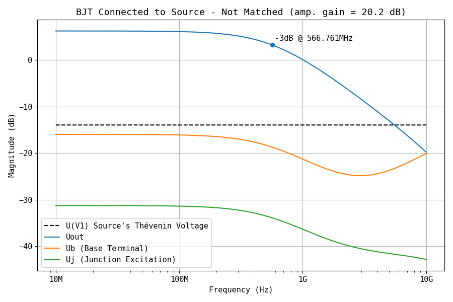
Figure 8 shows the voltage Ub at the base terminal, the output voltage Uout at the output load, and the internal base-emitter excitation voltage Uj. The configuration exhibits a gain of 20.2 dBV (a voltage gain, as the source and load impedance are different), and it is possible to see the cutoff frequency at ~566 MHz.
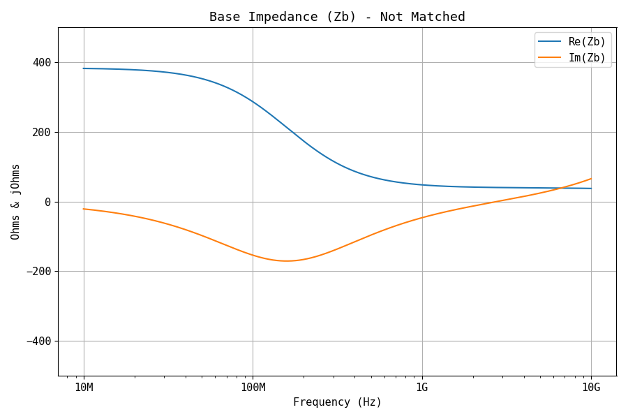
The impedance looking at the base of the transistor is complex and variable over frequency, revealing that its behavior is far from the voltage-sensor approximation usually assumed in low-frequency designs, as seen in Figure 9.
Besides the elements that impact the base impedance directly - like the series rb and LB, and the Cbe capacitance - the base-collector capacitance Ccb is transformed by the collector's current source (through the model's transconductance), impacting the input impedance in a nontrivial way (Miller Effect).
It is clear that the output signal magnitude will be proportional to the voltage Uj, as it is the driving factor for the output current.
Accordingly, it is correct to assume that maximizing the power at the base-emitter dynamic resistance re leads to maximum output by the simple fact that Uj will also be at maximum given Ohm's Law Pj = Uj 2 / re.
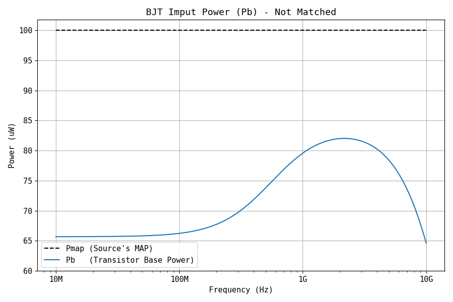
Figure 10 shows a SPICE plot calculating the power delivered to the transistor's base in the unmatched condition of Figure 6, defined as Pb = re(Ub.Ib°) where Ub is the voltage at the base and Ib° is the complex conjugate of the current entering the base.
The power entering the base is less than the signal source's maximum available power of 100 uW, showing that it is possible to achieve a higher voltage excursion on the re dynamic resistance internal to the model by matching the base to accept the source's Pavs.
That occurs because more power entering the transistor's base means that all the resistive elements of the small-signal model are dissipating more power due to the homogeneity property of linear systems, as will be demonstrated later in the article.
It is also interesting to notice that the power entering the transistor's base varies over frequency in a non-intuitive way. Later, we will see that the power at the junction, Pj, also has a complex-shaped frequency roll-off.
We now add an impedance-matching network between the transistor input and the signal source, with the task of transforming the base impedance, Zb, to 100 Ω. Matching should allow all the available power of the source to excite the transistor, increasing its amplification action.
Figure 11 shows a basic LC network in front of the transistor. The design of the matching network is not the main subject of the article, and that is a discipline in its own right. For the sake of this explanation, it is sufficient to know that the single LC section chosen can perform matching only in a single frequency.
For the sake of the example, we consider the BJT amplifier to be used to amplify a signal at 100 MHz, and the matching network inductance and capacitance, LM and CM, are calculated for that target frequency. One now expects that - at 100 MHz - all the available power from the signal source will enter the transistor's base terminal due to the voltage/current transformation provided by the network.
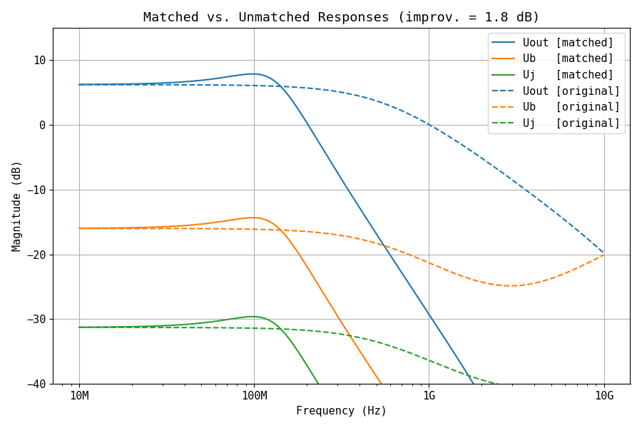
The output voltage, base terminal voltage, and junction excitation of the new setup are seen in Figure 12. For the operating frequency chosen, the output is larger by 1.8 dB - a 50% increase in power. The base terminal and junction excitation voltages are also higher exactly at 100 MHz.
As expected, the higher power entering the transistor's base allows the development of higher voltages in the internal nodes of the model, including the base-emitter junction voltage Uj. This higher excitation leads to a greater current modulation in the collector, thus generating a higher voltage at the load.
The matching network used - an L-shaped LC network - can perform the impedance transformation only at the designed frequency (the single frequency where the reactances act in combination to transform the base impedance to the generator's 100 R impedance).
Due to the LC network's low-pass nature (a series inductor + a shunt capacitor), the impedance transformation degrades above 100 MHz, worsening the mismatch and reducing the amplifier's bandwidth. This is one of the costs of impedance matching using reactive networks, where broadband responses are challenging to achieve and usually require high-order networks.
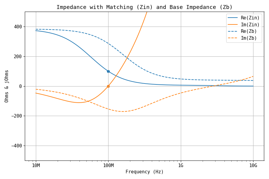
Figure 13 compares the input impedance at the impedance matching network (the impedance that the signal source experiences) to the base impedance. The LC circuit performs its job and transforms the impedance to exactly 100 R at 100 MHz.
Above the design frequency, the series reactance of the inductor (LM) dominates, worsening the matching condition. That is the reason the output of the amplifier drops sharply, as seen in Figure 12.
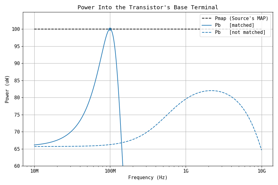
The power entering the transistor base is indeed optimized to the maximum available power of the source, as seen in Figure 14. The Pavs is achieved exactly at - and only at - the design frequency of the matching network.
Single-frequency matching is solely a characteristic of the simple LC matching network chosen. A broadband match - or a match at multiple frequency points - is achievable with higher-order matching networks.
For broadband applications, the same principle applies: designing the matching network to improve the match around the roll-off frequency can extend the usable bandwidth.
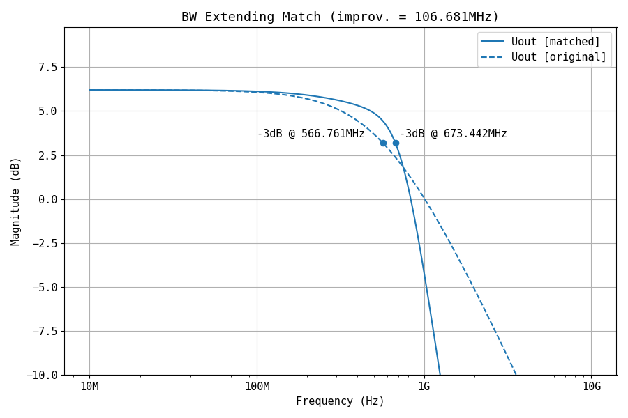
In Figure 15, the matching network was moved near the -3 dB frequency point of the amplifier's original response. Improving the match near the roll-off region can be used as a way of linearizing the frequency response, compensating for the natural low-pass behavior of the amplifier structure.
By simply calculating the matching network to be positioned in frequency 20% below the -3 dB (at around ~452 MHz), the overall broadband response of the amplifier is extended by ~106 MHz, from 566 MHz to 673 MHz.
The simulation demonstrates the effect for one specific circuit. The homogeneity principle proves this result in general, as it holds for any linear small-signal model with a single excitation port, regardless of topology.
The Homogeneity Principle
Depending on the field, the homogeneity principle is called the "scaling property" or the "principle of proportionality."
$$\tag{4} f(k \cdot \mathbf{u}) = k^n f(\mathbf{u})$$
A function is a homogeneous function, as defined by Euler, when the following holds: if each of its arguments is multiplied by a scalar, the function's output value is thus scaled by a power of that scalar. The power is then called the degree of homogeneity.
Equation 4 shows the principle in action, where k is the scaling factor and n is the degree of homogeneity. Let's now see how that relates to our problem of impedance matching.
To study and model the high-frequency behavior of the transistor, we relied on a small-signal model. The small-signal model is a linear representation of the transistor (or the whole circuit) at a specific DC operating point.
In practice, it means we treat the transistor as a linear circuit and the input as a perturbation over the biasing point. That is why it is called a "small signal" model, meaning the input and output signals must be small enough not to violate the linear assumption.
$$\tag{5} \begin{pmatrix} Y_{11} & Y_{12} & \cdots & Y_{1N} \\ Y_{21} & Y_{22} & \cdots & Y_{2N} \\ \vdots & \vdots & \ddots & \vdots \\ Y_{N1} & Y_{N2} & \cdots & Y_{NN} \end{pmatrix} \begin{pmatrix} U_1 \\ U_2 \\ \vdots \\ U_N \end{pmatrix} = \begin{pmatrix} j_1 \\ j_2 \\ \vdots \\ j_N \end{pmatrix}$$
A linear circuit with N nodes can be represented in matrix form and solved using the modified nodal analysis method, as shown in Equation 5, where Y is the system matrix, containing passive-element admittances and linearly dependent source gains; U is the dependent variable vector (unknown voltages and currents to be solved); and j is the excitation vector (independent inputs to the circuit).
$$\tag{6} f(j) = Y^{-1}j = U$$
Given the matrix representation YU = j, we can define a function f(j) that represents the circuit's response, without loss of generality, as seen in Equation 6. Since Y is a constant matrix (containing all internal admittances and dependent source gains), f is a linear operator.
$$\tag{7} f(k \cdot j) = Y^{-1}(k\cdot j) = k(Y^{-1}j) = k \cdot f(j)$$
If we scale the input source vector by a factor k, the new internal voltages U' are found by Equation 7, and this matches the form given in Equation 4, where n = 1. Thus, any linear circuit has homogeneity of degree 1 for the input-to-output voltage-to-voltage relations.
In practice, it means that if a linear circuit - of arbitrary complexity, with many internal dependent sources - is excited by an input voltage scaled by a factor k, all the internal circuit nodes will have their voltages scaled by the same factor.
By maximizing the excitation at the input port, the internal voltage Uj across the base-emitter junction is also maximized, and maximum current modulation on the collector will be achieved.
$$\tag{8} P_{in} = \text{Re} \left\{ \frac{|U_{b}|^2}{Z_{b}^*} \right\}$$
Given that the maximum voltage over the input port happens when the power entering the port is maximized, as seen in Equation 8, for a fixed linear network, any adjustment of the source parameters (matching) that results in a net increase in power delivered to the input port (Pin) must, by the Homogeneity Principle, result in a corresponding increase in the magnitude of all internal node voltages and branch powers.
The reason we kept some parasitics in the small-signal model used in the article, like the base-spread and diffusion resistances and base terminal inductance, is indeed to show that no matter the complexity of the circuit, homogeneity holds for small-signal analysis.
It is possible to demonstrate that the input-power-to-internal-voltage relation (here we are interested in the Uj voltage) follows homogeneity of degree 1/2, and that is shown with the following argument.
$$\tag{9} |U_i| = a_i \cdot |U_b|$$
For the article's small-signal model having a single input, the internal state is defined entirely by the voltage at the transistor's base terminal, Ub. Equation 9 shows that mathematically, mapping the internal state to the input voltage (where ai is determined by the circuit's admittance matrix and is frequency-dependent; the following argument holds at each frequency individually).
$$\tag{10} |U_{b}| = \frac{1}{\sqrt{G_{b}}} \cdot P_{in}^{1/2}$$
Equation 8 can be used to solve for the amplitude of base voltage, Ub, and that is shown in Equation 10, using Gb as the input conductance at the base terminal, where Gb = Re{1 / Zb*} = Re{Yb}.
$$\tag{11} g(P_{in}) = a_i \cdot |U_{b}| = a_i \cdot \frac{1}{\sqrt{G_{b}}} \cdot P_{in}^{1/2}$$
$$\tag{12} g(k \cdot P_{in}) = \left( \frac{a_i}{\sqrt{G_{b}}} \right) \cdot (k \cdot P_{in})^{1/2}$$
$$\tag{13} g(k \cdot P_{in}) = k^{1/2} \cdot \left[ \left( \frac{a_i}{\sqrt{G_{b}}} \right) \cdot P_{in}^{1/2} \right]$$
$$\tag{14} g(k \cdot P_{in}) = k^{1/2} \cdot g(P_{in})$$
By defining a function g(Pin) that maps the input power to internal states Ui, as seen with Equation 11, we demonstrate homogeneity of degree 1/2 to any internal state, as seen in Equations 12 to 14.
In short, doubling the input power increases all internal voltages by 41% (√2), regardless of the circuit's internal complexity.
Since impedance matching maximizes the power delivered to the transistor (as shown in Figure 14), and the homogeneity principle guarantees that maximizing input power maximizes all internal node voltages, matching directly amplifies gain.
Conclusion
The central argument of this article is that impedance matching is not an artifact of transmission line theory or a formality reserved for 50 Ohm systems; it is a direct consequence of how transistors convert input power into output signal.
Once we shift the perspective from voltage transfer to power transfer, it becomes clear: the signal source has a fixed amount of power available to deliver, and any mismatch at the transistor input leaves part of that power on the table.
We demonstrated this first with a simple resistive model, where the unmatched transistor received only 33 µW out of the 100 µW available from the source.
Moving to a realistic small-signal model with parasitics, we saw that the base power reaches its maximum precisely at the frequency where the match is designed and that repositioning the match near the rolloff frequency can be used to extend bandwidth.
The homogeneity principle ties the argument together in general terms.
Because the small-signal model is linear, scaling the input power by a factor k scales all internal node voltages by k^(1/2), and this holds for any linear network.
Maximizing the power that enters the input port - in this specific case, the transistor's base terminal - directly maximizes the voltage across the base-emitter junction and, consequently, the collector current modulation that produces gain.
In practice, this means that for any amplifier stage where gain matters, the designer should not rely on the transistor's high input impedance as a reason to skip matching. The available power is the hard limit, and impedance matching is the mechanism that delivers it.
References:
[1]⠀D. M. Pozar, Microwave Engineering.
[2]⠀https://batch.libretexts.org/print/Letter/Finished/eng-46038/Full.pdf
[3]⠀https://engineering.purdue.edu/wcchew/ece255s18/ece%20255%20s18%20latex%20pdf%20files/ece255Lecture_12_Feb22_BJT_Small_Signals.pdf
[4]⠀https://www.ittc.ku.edu/~jstiles/412/handouts/5.6%20Small%20Signal%20Operation%20and%20Models/The%20Hybrid%20Pi%20and%20T%20Models%20lecture.pdf
[5]⠀https://www.microwaves101.com/encyclopedias/maximum-power-transfer-theorem
[6]⠀https://en.wikipedia.org/wiki/Homogeneous_function
[7]⠀https://en-wikipedia-org.translate.goog/wiki/Nodal_analysis